Choosing between RF and optical automatic gain control
A challenge for equipment vendors is to help carriers deliver better services to their customers at the best price possible. For example, providers of video and data services using amplitude modulation-vestigial side-band (AM-VSB) optical transmission often must weigh how much fiber to use in any capital spend. A fiber to the home (FTTH) system promises lower operating costs, but carries with it higher home terminal equipment installation charges. To minimize these installation costs, equipment vendors incorporate automatic gain control (AGC) in their home terminals to adjust the ONTs’ RF levels without the intervention of the operator’s highly skilled technicians.
For easier deployment of FTTH across diverse geographies and fiber-optic architecture variants, a wide input optical range is highly desirable. For example, a larger AM-VSB optical dynamic range at 1550 nm can simplify co-deployment with content at other wavelengths having a wider dynamic range. The AM-VSB dynamic range is often the weak link in such a network design – any increase is welcome to better align the optical dynamic ranges. In particular, an improvement at the lower end of the AM-VSB optical window, enabled by increased use of QAM modulation, reduces the cost of transmission equipment such as EDFAs.
Even without co-deployment of alternate wavelengths, a wider range enables simpler network design and installation. New flexible FTTH deployments ask ONT equipment to accommodate optical input ranges as wide as -12 to +2 dBm, which is approaching 2X the optical dynamic range of older AM-VSB receivers.
For operators to enjoy this benefit in their rollouts, how AGC is implemented in the ONT receiver becomes critically important. Unlike the case of baseband light modulation, RF-modulated light requires special attention to distortion, noise, and other performance factors to preserve good customer experience. Optimization of relevant receiver parameters such as noise, distortion, and gain flatness forces unpleasant tradeoffs and hard choices that ultimately can increase design complexity and cost. Thus, one of the most important decisions a designer needs to make is the preferred AGC method within the ONT receiver.
AGC implementations: Optical or RF?
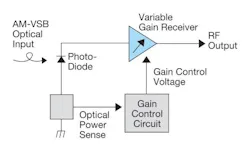
There are two primary types of AGC used in AM-VSB optical receivers. The most common today in a nominal receiver having about 10 dB of range is optical AGC, shown in Figure 1. Here the average level of incoming light power is detected by the receiver’s photodiode and is used by a control circuit to adjust the gain of the receiver. The optical AGC receiver can be thought of as a feed-forward open-loop correction scheme.
Conceptually, optical AGC is simple to understand - more light means the receiver gain should be reduced to hold the output level constant. Unfortunately, that’s about where the simplicity ends with optical AGC. Implementing it can be challenging, particularly when the input optical range is increased to save costs at the system level.
The problem with variable gain receivers with wide continuous adjustment range is that the relationship between the control voltage and amount of gain is usually a non-linear function whose characteristics change appreciably over temperature and typical manufacturing variances. The gain control circuit must map the optical power indicator into a unique control voltage with good accuracy. Such mapping was challenging, but achievable, for older optical input ranges; it becomes very daunting for wider optical input ranges, such as the -12 to +2 dBm range now contemplated.
During receiver design, distortion and gain flatness considerations are normally at odds with the goal of having a desirable relationship between gain and control voltage. The addition of this extra requirement forces tradeoffs that increase complexity and cost. For example, a micro-controller may be programmed to perform the gain-shaping function, but with the drawback of a clock being added in the proximity of the receiver. Additionally, any variations in the level of modulation on incoming light or of the receiver’s gain with temperature will not be reflected in the optical AGC scenario. As we said, optical AGC is an open-loop correction scheme.
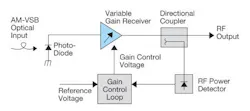
The other approach is RF AGC, depicted in Figure 2. Here the RF signal leaving the receiver is directionally detected and sent to a feedback control loop containing an integrator. The control loop can easily be designed to absorb the non-linear relationship between the control voltage and the receiver gain; they are effectively absorbed by the high gain of the integrator in a closed-loop feedback system. In this case, device parameters that affect gain and change with time and temperature are corrected. Instead of the difficulty of open-loop gain alignment to achieve RF output control, the job becomes designing a temperature-compensated RF power detector – a much simpler task with surprisingly good results at low cost from multiple sources.
A few complexities of RF AGC are worth mentioning, however. The broadband RF power detector needs to have directional qualities to isolate the outgoing signal from reflections that may come back from impedance mismatches after the receiver, such as from poorly maintained customer premises. Without this directivity the RF detector will, in the presence of reflections, give readings that will lead to an improper output level exiting the receiver.
The other problem with RF AGC is perhaps more troubling. As operators change their content lineup from legacy analog to QAM and make further adjustments to support increased upper spectrum limits, the servo action of the loop will force a change in the RF level per channel. Hence, the RF output level per channel, so central to customer premises architecture, is muddied by possible future changes to content and frequency plans.
Fortunately, it’s possible to bandpass filter the signal after the directional coupler, which prevents the power detector from seeing changes in content. Assuming the content within the filter pass-band will not change, the RF AGC system can be designed so the RF output level per channel would not appreciably change with signal changes outside the bandpass filter.
Currently, most operators favor optical AGC due to its perceived simplicity and separation of output level from the issue of channel planning. But as new systems start with less analog content with wider optical input ranges, the advantages of RF AGC may become more attractive in the push to minimize total costs.
Changing the gain
Not all gain modifying circuits are equal. One of the most important distinctions is between those that operate continuously as a function of their control voltages or currents and those that have discrete steps over at least part of their range. The latter can be easily designed but are highly problematic with digital content, where bit errors may occur during the brief time during which the receiver gain is being switched.
These undesirable steps in gain usually force the design into one of two techniques available for true continuous gain control over the full range. Figure 3 shows how a variable gain receiver can be built by locating a variable attenuator between an input TIA stage and a post-amplifier stage.
constant gain stages.
One traditional approach for the variable attenuator uses PIN diodes, whose RF resistance can be continuously controlled over a wide range by a DC bias current. PIN diodes are specifically intended for this problem and are available from multiple vendors at reasonable cost. The use of multiple PIN diodes can lead to an attenuator with >30-dB RF control range and good distortion and dynamic gain flatness characteristics.
The alternative to PIN diodes is to use a FET as the variable resistor element. FETs are used in very high volume as switching elements, but can also be used in a continuously variable attenuator. FETs can make very consistent on/off switches with impressively low distortion; however, distortion inconsistency in the middle of their resistance range becomes a challenge for device fabricators and circuit designers. In addition, FET attenuators can struggle to simultaneously achieve both wide attenuation range and the consistent performance so critical for optical AGC.
The clear advantage of FET attenuators, however, is that they offer the possibility of a lower cost, single die design.
Forward thinking
Simple manual approaches for gain control used in previous optical AM-VSB deployments may not suit tomorrow’s networks. An automatic gain adjustment routine promises reduced installation and maintenance costs.
As fiber moves closer to the subscriber, the importance of how gain control is implemented in the ONT receiver becomes increasingly relevant in the quest for lower overall costs. A forward-thinking AGC approach that accommodates a growing optical input range as well as analog and digital content types will help operators benefit from their FTTH investment over a longer time horizon. RF AGC can provide clear advantages in performance and cost when operators want to increase their optical input windows for ease of installation and system design.
Chris Day is technical director of CATV/FTTH product solutions at TriQuint Semiconductor.


