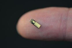
With silicon photonics still gathering significant attention, Dutch startup EFFECT Photonics is keen to show that there's still life in indium phosphide (InP) integration. The company has introduced a line of optical transceivers for 100-Gbps 20- to 80-km metro access applications based on a fully integrated InP DWDM system on a chip (SoC).
A spin out of the Technical University of Eindhoven, EFFECT Photonics has developed the SoC over the past five years, according to CEO James Regan. The SoC integrates both passive and active elements, including tunable lasers (see photo above). The company's proprietary integration process begins with active elements on the InP wafer. Etching prepares the wafer for passive elements, which are added via regrowth. The result is an efficient and economical packaging technology for such optical module formats as CFP and CFP2, as well as smaller formats, Regan says.
Optical functions the company can integrated include:
- tunable lasers
- arrayed waveguide grating (AWG) multiplexers
- high-speed photo-detectors
- high-speed modulators, including single- or multi-stage Mach-Zehnder modulators (MZM/MZI)
- power taps and splitters
- channel monitoring.
The company announced Series A funding this past February, led by b-to-v Partners and including the Brabant Development Agency (BOM) and Optidob.
The company's initial optical modules, now sampling, target DWDM-based metro applications such as fronthaul, backhaul, and data center interconnect in a 10x10-Gbps format using direct detection. The company also has an eye on NGPON2 applications, Regan says.
"100 Gbps over 40 km to 80 km is a significant market opportunity that has no cost-effective solution today. This is the next battleground for 100G solutions," said Andrew Schmitt, founder and analyst at Cignal Al, via an EFFECT Photonics press release.
For related articles, visit the Optical Technologies Topic Center.
For more information on optical modules and suppliers, visit the Lightwave Buyer's Guide.
