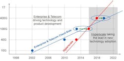
The rapid global growth in cloud computing is driving massive demand for high-capacity data center infrastructure. While fixed and mobile broadband services primarily drove recent network bandwidth upgrades, the latest wave derives from a rapid increase in machine-to-machine traffic due to an expansion in server virtualization and software defined networks (SDNs). The result is a dramatically different growth rate, illustrated in Figure 1, that is outpacing consumer traffic expansion.
Similarly, the telecom/enterprise market traditionally has led early adoption and hence influenced the development of new module technology. However, the new hyperscale growth of data center interconnects has changed the dynamic of module innovation and deployment as well.
Hyperscale data centers are changing the game
Telecom/enterprise applications first adopted 100G technology in the form of CFP modules. Data centers generally did not adopt 100G interfaces until the technology matured and evolved towards denser, lower power interfaces, particularly in the form of QSFP28 modules.
However, as the hyperscale data center market scales to keep pace with machine-to-machine communications needs, data center operators have become the first to demand transmission modules for data rates of 400G and beyond. The drive to meet this requirement will lead to a couple of fundamental shifts in the market. First, as the data centers replace telecom/enterprise as the early adopters of new technology, that emerging technology will reflect their requirements. Second, those requirements are radically different from those typically associated with telecom. The telecom market generally required specific environmental, reliability, and interoperability/standardization features. But 400G optical modules will be focused on the needs of the data center and its associated challenges: high faceplate density, low power consumption, ever lower cost per bit, and reliable large-scale manufacturing capabilities.
Smaller, faster, lower cost per bit optical modules
Meeting these different requirements will take a variety of strategies. To enable maximum density, data center modules are ideally sized such that the number of modules in one rack unit (1RU) is aligned with the throughput of the switch ASIC inside that unit. For example, in existing 100G data center switches, 32 QSFP28 modules fit in 1RU, which aligns with a 3.2-Tbps switch ASIC. This trend will continue as switch ASICs scale to approximately 12-14 Tbps interfaces on a single 1RU faceplate.
The concept of multiple lanes to increase bandwidth has been widely used for 20 years in line-side transmission networks since the advent of DWDM. Adoption in shorter reach data center applications has been more recent, starting with 40G and now 100G modules using either multiple fibers or WDM. Future modules will need to strike a balance between number of lanes, bandwidth (baud rate), and bits per symbol to fit within the allowed size and power envelope while achieving the lowest possible cost. Generally, the fewer lasers and receivers required, the lower the cost will be.
There are several core technologies that will enable 400-Gbps interfaces, as well as higher data rates, within these balanced design parameters. One is the use of higher order modulation. Today’s data center interconnect transceivers are based on non-return-to-zero (NRZ) modulation, which transmits one bit per symbol. The next level of modulation provides four-level pulse amplitude modulation (PAM4), which transmits two bits per symbol, therefore doubling the data rate without doubling the required overall bandwidth over conventional NRZ (see Figure 2).
The consequence for this move to additional levels per symbol is a requirement for higher signal-to-noise ratio (SNR). To achieve higher SNR, PAM4 components require greater linearity in the modulated laser source and detector, higher extinction ratio, low relative intensity noise (RIN), greater output power, and higher responsivity. These characteristics will drive the development and choice of components to provide the necessary performance while still achieving the cost and density needed, even as hyperscale applications require enhanced loss budgets that extend beyond the standard 3-5 dB.
Components and packaging
For example, one of the key components that drive performance is the laser and its modulation. In existing <2 km 100G NRZ applications, both directly modulated lasers (DMLs) and externally modulated lasers (EMLs) provide acceptable performance. In the former, the drive current to the DML is varied to provide different levels of light amplitude representing the 1s and 0s. EMLs have a fixed laser driver current; the light is modulated by varying the voltage to the monolithically integrated electro-absorption modulator or Mach-Zehnder modulator, which then modulates the laser light.
In moving from NRZ to PAM4, the variation of the DML drive current intensity leads to a lack of linearity, additional noise, and low extinction ratio. There are emerging DML technologies that promise improved performance through a photon-photon resonance (PPR) effect between the distributed Bragg reflector (DBR) and the distributed feedback (DFB) laser structures. The PPR effect extends the modulation bandwidth beyond that of the DFB alone. However, the additional complexity of the grating and electrode structure will increase the component cost and reduce yield, while the reliability risks will remain a concern in these aluminum-containing structures. Therefore, it is too soon to determine if these devices can compete with the maturity, performance, and lower cost that EML technology delivers.
In addition to high performance, 400G transceivers also must support low cost per bit and the ability to reliably and efficiently scale to high-volume manufacturing. This has driven innovation in transceiver component design with a focus on leveraging the advantages of integration, automation, wafer-scale production, and non-hermetic packaging.
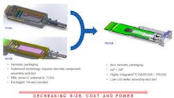
Such innovation is apparent in the receive optical subassembly (ROSA) and the transmit optical sub-assembly (TOSA). The cost of TOSAs and ROSAs is driven by the assembly of discrete components, alignment, burn in, and high cost of yield loss at the subassembly/module level. To address this, new TOSA and ROSA designs are emerging that leverage the use of wafer-level integration in assembly, packaging, and testing, based on both silicon photonics and complementary techniques within indium phosphide (InP).
Silicon photonics offers the use of mature, large-scale processes compatible with complementary metal–oxide–semiconductor (CMOS) technology, today’s standard for building integrated circuits, to precisely generate thousands of optical components on a monolithic substrate in a fully automated manufacturing environment. Enabled elements include optical waveguides, splitters, couplers, modulators, detectors, multiplexers, and demultiplexers.
In practice, silicon photonics components are defined through CMOS processes that involve lithographic patterning, material deposition, removal, and modification. These processes are repeated to build up the desired structure of the optical components and circuitry. Once complete, the wafer containing a patterned grid of devices can be burned in and tested before singulation. Testing at this comparatively earlier, lower cost point in the manufacturing process improves yield versus conventional photonic device manufacture.
Unfortunately, silicon has two photonic design challenges. A weak electro-optic effect makes silicon active elements like modulators relatively complex. Silicon’s indirect bandgap structure also has not produced effective gain structures for lasers or optical amplifiers.
To resolve these issues, materials such as InP with higher electro-optic effect and well characterized optical lasing and amplification properties must be integrated into the monolithic silicon component. There are several ways to do this, including optical coupling between InP silicon waveguide edges, fiber coupling of the laser/modulator source to the silicon, and flip-chip integration of the laser to the silicon. The wafer-level integration of InP performance with the low-cost aspect of silicon photonics provides a platform that is well positioned to address the cost and density needs of the hyperscale market.
Silicon photonics offers additional benefits as well. For example, historically TOSA/ROSAs have been hermetically sealed to protect materials and free-space optics from environmental contamination that could reduce performance and reliability. Sealing is a time consuming and expensive process. Silicon is "self-hermetic" and therefore does not require hermetic packaging. This attribute greatly reduces the constraints on the design, materials used, and fabrication complexity required to build optical subassembly (OSA) packages.
Some materials, including InP, will still need hermetic protection. But there are several ways to achieve this cost-effectively on a chip or wafer level that preserves wafer-level packaging and test. As a result, such OSAs use less material, require fewer process and test steps, and produce higher yields through final assembly and burn-in, all of which results in lower cost.
Silicon photonic OSAs also can be made small enough to be assembled into smaller transceiver form factors that can increase faceplate density. Figure 3 illustrates an example of the evolution of hermetically sealed TOSAs and ROSAs to InP and silicon photonics based optics.
Building the foundation for future data center transceivers
In summary, data centers are leading the migration to 400G interconnects, given the high growth in machine-to-machine capacity demand. The reduced size, low cost, and low power requirements of data center applications necessitates performance-oriented components that support the use of higher-order modulation, simultaneously with highly integrated and wafer-level packaging techniques to achieve critical low device costs.
The use of silicon photonics transforms discrete components and InP elements into monolithic structures with small, less complex packages. Component developers have begun to merge industry-proven InP laser/modulator sources with wafer-level silicon photonics integration and packaging techniques to provide the required performance and low cost, power, and size. Combine such designs with high-volume manufacturing and testing experience, and the new generation of components creates a technology foundation that will enable low-cost transceivers for the emerging data center market.
Justin Abbott is senior product line manager for next generation products and David Horn is director, datacom product and technology strategy, at Lumentum.


