III/V and Silicon – Friends or Foes for 400 Gigabit Ethernet?
The advent of 100G in the QSFP28 form factor finally signaled the arrival of 100 Gigabit Ethernet (GbE) into the network mainstream. This development was not driven by classic telecom network operators, but rather by hyperscale data center operators and internet content providers. These new players specified clear targets for density per rack unit, matching the speed of switching silicon (e.g., 3.2 Tbps per 1RU), and reach classes suited to data center deployments. This last requirement led to several options, including a 500-m PSM4 and 2-km CWDM4 interface in addition to the classic multimode short-reach (100 m) and single-mode long-reach (10 km) interface.
Moreover, the space has seen the first colored pluggable 100G line-side optical module for short-reach data center interconnect (DCI) via PAM4 modulation. The optical transceiver eliminates the transport layer in these applications while maintaining a versatile pluggability in the switch (assuming a higher power consumption per port can be accommodated in the design).
Despite new proposals for 100G form factors, like the µQSFP, the QSFP28 is widely believed to be the mainstay for 100G for interconnects inside of the data center.
Meanwhile, the market now must consider what comes after 100G to accommodate an ever-growing amount of machine-to-machine communications (think Internet of Things) and streaming high-definition video. To enable such applications, the next generation of higher-speed interfaces will have to continue to comply with many of the 100G objectives, including higher density per rack unit, matching the face-plate capacity to new switching silicon of 6.4 Tbps and 12.8 Tbps, and low device cost. The market looks to these new interfaces to support changes in intra data center connectivity toward fewer layers in the top-of-the-rack (TOR), the use of leaf and spine switching architecture, and the introduction of larger switches.
The first generation of 400GbE grey interfaces, in a CFP8 form factor, is currently under development. Yet with a target power consumption of around 12 W and a size comparable to a 100G CFP2, the CFP8 would enable only a doubling of face-plate density compared to QSFP28. On the optical side, 400GbE is transmitted as 8x50G PAM4 with 16x25G I/Os on the host side, naturally requiring PAM4 signal processing on the line and a gearbox functionality between line and host. While such an approach might see limited use by early adopters of next-generation network processing units or switching silicon, the industry consensus is that the CFP8 will become merely a footnote in the development of 400GbE, since it doesn’t address the pain point of hyperscale data centers.
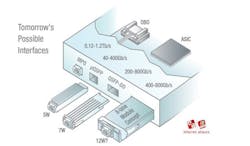
Figure 1 shows other currently discussed formats. While Microsoft showed early support for onboard optics on the assumption that a suitable pluggable format was out of reach, the QSFP-DD (double density) and another, as yet unannounced form factor are shaping up to deliver quadruple density and lower costs based on 4x single-lambda PAM4 modulation with direct detection.
With single-lambda PAM4 DSPs already in development, what are the crucial building blocks for optics going forward that would enable scalable, high-volume, shorter reach 400G interfaces for applications ranging from a few hundred meters up to 80 km?
The Choice of Material
A large debate continues to rage within the industry about which material system will best enable the intra- and inter-data center interconnect market: III/V material (such as InP and GaAs) or silicon photonics? Companies that own the respective technologies have driven this discussion, which has often relied more on political reasoning rather than an objective evaluation of technological features.
But is "silicon photonics or III/V" the right question to ask? A well justified argument from the III/V side is that the silicon photonics platform is missing a gain block, which is eventually realized in III/V. Therefore, the question should be phrased differently: Which is more suitable – III/V or silicon photonics + III/V? Put another way: If a III/V gain block is needed anyhow, why should we use silicon at all? Can III/V be the sole material?
Indeed, the III/V component library comprises all of the essential building blocks for direct detection systems, from lasers and amplifiers to modulators and photodetectors. However, as demands eventually drive a move to (coherent) polarization-multiplexed transceivers, a polarization beam splitter/combiner (PBSC) and a polarization beam rotator (PBR) become additional essential building blocks. Although academic publications report that such building blocks can be realized in InP as well, such InP components usually don’t appear in commercial applications. That’s because InP manufacturing processes are less mature than those of silicon, which has a strong negative impact on yield. As a consequence, the manufacturing processes of InP need to be continuously monitored and readjusted, and PBSC and PBR appear to be particularly prone to those dynamics.
For this reason, integrated coherent receiver (ICR) assemblies in InP and InP coherent transceivers mainly rely on off-chip PBSC and PBR structures, typically based on rather large planar lightwave circuits (PLCs) or even discrete optics.
The silicon photonics platform, on the other hand, features both PBSC and PBR in their design kit library as well as modulators and photodetectors. But, as mentioned before, the silicon photonics library lacks a gain block. For this reason, silicon photonics integrated modulator-receiver-assemblies are typically either fed by an external laser source (as is the case for coherent interfaces based on silicon photonics) or use hybrid integration of III/V on silicon as demonstrated in QSFP28 based 100G short-reach products.
Would a combination of InP and PLC/discrete optics deliver a small form factor, high-volume 400GbE module? With the prospect of ever-increasing integration densities, a pairing of a highly integrated, small footprint III/V photonic integrated circuit (PIC) with a rather bulky PLC or discrete optics seems like a compromised approach. In terms of integration density, a combination of silicon photonics and III/V material appears to be the more suitable combination.
But what would such a combination of III/V and silicon look like, as many building blocks can be implemented in either of the two material systems? One can look at three approaches:
- The approach of the silicon fundamentalist: Build everything that you can in silicon – waveguides, couplers, splitters, modulators, polarization beam splitters/combiners and rotators, and photodiodes. Use III/V only as a gain block – even realize the laser resonator in silicon. However, this approach would not result in the highest performance, as a hybrid III/V-Si laser is never as efficient as a mature III/V laser. However, this approach could be particularly interesting when price/bit is the dominant decision driver, such as for shorter-reach interconnects along the lines of 100G CWDM4 or 100G DWDM PAM4.
- The approach of the InP fundamentalist: This fundamentalist would be forced to ally with the silicon foe due to the increasing demand for integration density. However, such an alliance would be a natural evolution from the current state-of-the-art for InP companies. A silicon photonics PIC with PBSC and PBR would replace the bulky PLC or free-space optics. All other building blocks would be realized in InP.
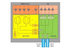
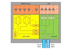
- The neutral approach: Use the two platforms for what they can do best. InP Mach-Zehnder modulators are superior to those in silicon in terms of modulation efficiency (Vpi) and similar in bandwidth and size. Therefore, transmitter IQ-modulators, light sources, and amplifiers would be realized in III/V, while PBSC and PBR would be realized in a silicon photonics PIC. This PIC also could host all the building blocks of a coherent receiver, including 90° hybrid, balanced photodiodes, and on-chip PBSC and PBR, all at a total die size below 0.1 mm². In this way, highly energy- and cost-efficient multi-wavelength transceiver assemblies could be realized within the smallest footprint (see Figure 2).
A Look Ahead
The joint leverage of silicon photonics and III/V is an important path toward reducing the price per gigabit in the mid-reach market. However, since packaging is one of the largest cost drivers, more and more functions need to be combined in next-generation transceiver assemblies. At first, next-generation assemblies need to feature a large channel density to keep the relative assembly cost low. Also, modulator drivers and receiver trans-impendence amplifiers need to be co-packaged with the PIC, both reducing total cost and overall footprint.
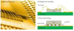
As the number of channels per package increases, a switch from the traditional butterfly package to ball-grid-array (BGA) based packages is inevitable (see Figure 3). Within the package, the large number of electrical interconnects will require a switch from wire-bonding to flip-chip bonding (see Figure 4). However, how to do this is an unsolved challenge for InP, as its critical process temperature is below the requirement for conventional flip-chip bonding. This might be a turning point to put even more emphasis on photonic integration in silicon.
What is further on the horizon of photonic integration? The Holy Grail would be a single housing in which all optical and the essential electrical drivers are co-packaged in a non-hermetic form. Among those components could be new building blocks for optical signal preprocessing to reduce the workload and power consumption of the DSP ASIC, e.g., optical dispersion compensation, input polarization rotators, and the like. The boundary between direct-detect and coherent technologies in the future might shift further to enable coherent-only transmission outside of the data center. The industry certainly might see 400GbE coherent variants of the aforementioned form factors (CFP8, QSFP-DD), although questions of power consumption and cost will remain looming over coherent technology before it can really claim the sub-80-km market fully for itself.
Dr. Robert Palmer is senior lead engineer at Coriant R&D GmbH, a position he has held since July 2014. His research interests include integrated optics and coherent communication systems.


