Efficient optical performance starts with the proper mating of driver to diode. Here's a look at the basics.
Justin Redd and Quentin Tan
Maxim Integrated Products
Interfacing laser-driver circuits with commercially available laser diodes at high data rates can be a complicated and frustrating task. The three major pieces of the laser interface puzzle include the output circuit of the laser driver, the electrical characteristics of the laser diode, and the interface between them (which is usually implemented using a printed circuit board). This application note first discusses the characteristics of the laser driver, then brings it together with the laser diode in a discussion of the printed-circuit-board interface. Although this application note is intended to be general in nature, specific examples will focus on Maxim's 2.5-Gbit/sec telecommunications laser drivers.
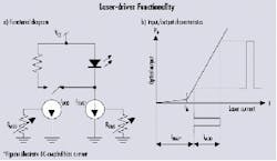
The primary function of a laser driver is to provide appropriate currents for bias and modulation of the laser diode (see Figure 1). The bias is a constant current that pushes the laser-diode operating range beyond its threshold value and into the linear region. Modulation is an alternating current that is switched on and off in synchronization with the input voltage waveform. Ideally, the bias current should track the changes in threshold current and the modulation current should track the changes in slope efficiency.
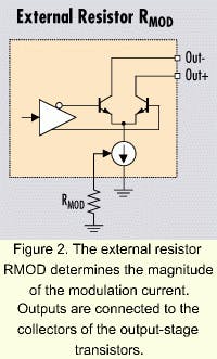
Laser drivers such as the MAX3867 and MAX3869 are designed to drive common-anode laser diodes. The bias current can be set between a minimum value (typically 1-5 mA) and the maximum value (typically 60-100 mA) by using an external resistor.Figure 1. Laser drivers provide the appropriate currents for bias and modulation of the laser diode. WhILe these ILlustrations highlight DC-coupled applications, AC coupling also can prove advantageous.
It is important to maintain a constant impedance at the cathode of the laser diode so the load on the high-speed output circuit versus frequency will remain stable. An unstable load on the output circuit may cause reflections or ringing that will degrade the quality of the optical waveform. The shunt capacitance associated with the biasing current source results in an impedance (ZBIAS) that is a function of frequency. To minimize the effect of this impedance variation, an external isolation inductor (or ferrite bead) is generally connected between the cathode of the laser diode and the bias circuit. This inductor has no effect on the DC bias current but appears as a high impedance to the modulation current.
Today's optical-communications systems require improvement in operating speed, transmission distance, and power consumption. Implementation of these improvements requires faster edge speeds, increased modulation current, and lower supply voltages. Therefore, the design of the laser driver and corresponding interface to the laser diode are important issues for high-speed fiber-optic communications design.
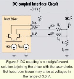
DC coupling between the driver and laser provides a simple, straightforward interface solution (see Figure 3). But when the power-supply voltage is decreased to 3.3 V, the headroom for the driver may not be enough to enable fast switching. ("Headroom" refers to the difference between the VCC supply voltage and the sum of the individual voltage drops along a single circuit path.) Headroom calculations for circuits that contain a laser diode must include voltage drops due to the laser itself as well as the transient voltage drop due to the parasitic inductance of the laser package and the voltage drop across the damping resistor, RD.
Typical long-wavelength Fabry-Perot-style laser diodes require forwaRD bias voltages on the oRDer of 1.2 to 1.8 V. This forwaRD bias requirement is the sum of the bandgap voltage and the voltage drop across the equivalent series resistance of the laser diode. The equivalent series resistance of this type of laser is typically between 4 and 6 ohms.
The transient voltage drop is due to fast switching currents across the parasitic inductance associated with the laser package. Its magnitude can be loosely approximated by VL = L Di/Dt. If we assume a typical laser package has a parasitic inductance of about 1.5 nH, a maximum modulation current of 60 mA, and a 20%-80% rise/fall time of 80 psec (for 2.5 Gbits/sec), then we can calculate an approximate value for VL. (Note that Di during the 20%-80% rise time is approximately 60% of the total modulation current or 0.6x60 mA = 36 mA.) Using the above assumed values, VL Δ (1.5 nH)(36 mA/80 psec) = 0.68 V.For an example of headroom calculation (for the DC-coupled interface of Figure 3), consider a packaged laser diode with a maximum forwaRD voltage VF of 1.6 V. We will also assume a package parasitic inductance of 1.5 nH, and a 60-mA modulation current with 20%-80% edge speed of 80 psec, resulting in VL = 0.68 V. Finally, we must include the voltage drop across the series damping resistor RD, which is IMODRD = 1.2 V (assuming RD = 20 ohms). The resulting voltage at the driver output pin can be as low as VLOW = VCC - 1.2 V - 0.68 V - 1.6 V = VCC - 3.48 V, making 3.3-V operation very difficult.
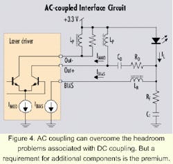
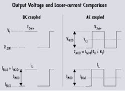
This headroom problem can be improved by AC-coupling the driver to the laser diode, which is accomplished by adding a series capacitor, CD, and pull-up inductors, LP, as shown in Figure 4. AC-coupling voltage drops are as follows: (1) The AC voltage drop across the laser diode is only a function of the voltage drop across its equivalent series resistance (not the bandgap), which is equal to the modulation current times the equivalent series resistance; (2) the transient voltage drop due to parasitic inductance remains unchanged from the DC example; and (3) the voltage drop across the series damping resistor, RD, is equal to one-half the modulation current times RD.This last point (voltage drop across RD) can be understood by considering the current through the AC-coupling capacitor, CD, and the currents at the circuit node, which includes the cathode of the laser diode (see Figures 4 and 5). The current through CD must have an average value of zero and a total peak-to-peak current swing of IMOD.
To satisfy these conditions, one-half of IMOD must flow into CD (from the laser) during an optical high output and one-half of IMOD must flow out of CD (towaRD the laser) during an optical low output. The current through the laser, IL, is then equal to the sum of the currents flowing out of the circuit node at the cathode of the laser diode. That means that during an optical high output IL equals IBIAS + IMOD/2 and during an optical low output IL equals IBIAS - IMOD/2. The difference between IL during an optical high output and IL during an optical low output is then (IBIAS + IMOD/2) - (IBIAS - IMOD/2) = IMOD.Figure 5. The differences between output voltage (VOUT+) and laser current (IL) for DC- and AC-coupled interfaces are apparent.
The example headroom calculation for the DC-coupled interface can now be modified using the AC-coupled changes. For the AC-coupled case, we assume the equivalent series resistance of the laser is 5 ohms, and the resulting headroom calculation is VLOW = VCC - (60 mA)(5 ohms) - 0.68 V - (60 mA/2)(20 ohms) = VCC - 1.58 V. For VCC = 3.3 V, that leaves 1.72 V of headroom for the driver, which enables fast current switching in the driver output stage.
The disadvantage of the AC-coupling approach is that additional discrete components are required. These additional components include a coupling capacitor and pull-up inductors or resistors for driver-transistor biasing (see Figure 4). Because these components are in the high-speed signal path, they may cause signal distortion. For this reason, the use of good high-frequency PC-board layout techniques is critical.
The AC-coupling capacitor will introduce a low frequency cutoff, which may affect the pattern-dependent jitter performance of the system. To reduce the pattern-dependent jitter caused by long strings of consecutive identical bits, the value of the AC-coupling capacitor should be as large as possible. Designs that include Maxim's 2.5-Gbit/sec laser drivers generally use an AC-coupling capacitance value between 0.056 and 0.1 µF.The pull-up inductor or resistor is required in AC-coupled laser interfaces to keep the output driver transistor properly biased. (Small ferrite beads are generally used for the inductive pull-up.) There are two disadvantages of using a resistor (versus an inductor) in this application. First, a resistive pull-up (Rpull-up) creates a current divider with the rest of the laser circuit, taking part of the modulation current from the laser. That does not happen with an inductor. Second, inductive pull-ups increase the headroom by allowing the average voltage at the output to be VCC (see Figure 5) instead of VCC - (IMOD/2)Rpull-up, as would occur with a resistive pull-up.
The specifics of the interconnection between the driver and the laser diode depend on the separation distance. If this distance is <2 mm (for 2.5 Gbits/sec), transmission lines are unnecessary and the priority is to reduce the parasitic elements as much as possible.
The inductive load caused by the lead- and bond-wire inductance of the laser package may need a compensating RC shunt network (see Figure 4), consisting of a resistor (RF) and a capacitor (CF). The purpose of the RC shunt network is to cancel out the parasitic inductance, thereby maintaining a constant load impedance, which results in a reduction of overshoot and ringing.The series damping resistor (RD) serves the dual purposes of damping reflections that cause output distortion and creating a stable load. Load stabILity is improved because the load presented by the laser may vary by ±20% or more from the nominal value of about 5 ohms (±1 ohm/5 ohms Δ ±20%), whILe the combined load presented by the laser and RD will vary by only ±4% (±1 ohm/25 ohms Δ ±4%). Since package inductance varies for different lasers, the component values for the shunt network may need to be adjusted for optimum operation. Also, it is important to note that the bias inductor is connected directly to the cathode of the laser (rather than the other end of RD), so that RD will not cause headroom problems in the bias stage of the driver.
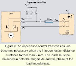
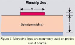
When the interconnection distance becomes >2 mm, an impedance-controlled transmission line is required to interface the laser to the driver (see Figure 6). Figure 7 represents the cross section of a microstrip line, which is commonly used in printed circuit boards. The characteristic impedance, Z0, is estimated bywhere W is the width of the top conductor, T is the thickness of the top conductor, H is the thickness of the dielectric, and er is the dielectric constant. For a 25-ohm microstrip line built on conventional FR4 material (er = 4.7) with a height of 356 micron, a line width of about 1.3 mm results.
For high-speed differential drivers, it is important to maintain a balance between the loads on the two outputs. The loads must be balanced in both the magnitude and the phase of the load impedances (see Figure 6). To maintain balanced load impedance, each output is set up to drive an equivalent 25-ohm load; the positive output drives a transmission line terminated on the load end to VCC through a matching resistor/laser diode (a 25-ohm combined load), and the negative output of the driver is connected to VCC through a 25-ohm resistor. Decoupling capacitors provide AC-shorts from the laser anode to ground and from the 25-ohm resistor on the negative output to ground.
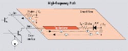
The high-frequency path can be divided into several portions (see Figure 8). Portion A is from the driver positive output through the top conductor of the transmission line to the termination resistor, whILe portion B is the termination resistor and the laser diode. Portion C is the decoupling capacitor to ground. Portion D is from the decoupling capacitor-ground contact to the transmission-line image. Portion E is the transmission-line image on the ground plane. Portion F is from the transmission-line image to the ground contact of the DC-coupling capacitor at the negative output; portion G is the decoupling capacitor at the negative output; and portion H is the resistor at the negative output.Figure 8. The high-frequency path can be divided into several portions. It is important to provide good decoupling from VCC to ground at both the passive and negative outputs.
Because the high-frequency return path includes the ground plane, it is important to provide good decoupling from VCC to ground at both the positive output and the negative output. The decoupling at the positive output (portion C) ensures a return current (along the transmission-line image) for proper transmission-line operation, and the decoupling at the negative output (G) enables a current return to the negative output. It is always a good practice to use physically small capacitors for high-frequency performance in these decoupling elements. It is also important to maintain an uninterrupted ground connection between these two capacitors (D, E, F).
It is desirable to keep portions B, D, F, and H (that are not transmission lines) as short as possible to reduce the propagation delay between the two driver outputs. That's because the propagation delay can be translated into unbalanced phase termination between the outputs of the differential pair. One way to improve this situation is to select physically small termination resistors to keep the ground contact of the decoupling capacitors as close to the transmission line as possible. It is also necessary to minimize the length of the non-transmission-line portion of the printed circuit board at the driver output pins.
Justin Redd, Ph.D., electrical engineering, is a senior member of the technical staff for the high-frequency/fiber-communications group at Maxim Integrated Products (Beaverton, OR). Quentin Tan, Ph.D., electrical engineering, is with the high-frequency/fiber-communications group at Maxim Integrated Products.
