Integrated-circuit manufacturers are focused on the natural solution to the driver requirements of the future.
YUAN MA and KEN TIMKO, Agere Systems
Multichannel high-voltage integrated-circuit (IC) amplifiers are targeted at the emerging field of optical micro-electromechanical systems (MEMS), which is generally referred to as optical/optoelectronic systems with one or more micro-mechanical elements (such as micro-mirrors).
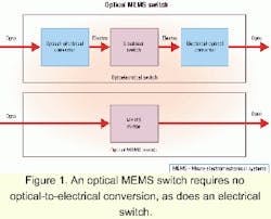
Optical MEMS is the keystone for all-optical networking. Instead of converting optical signals to electrical (O/E conversion) for processing/switching, and then converting back to optical conversion again, an optical MEMS switch requires no O/E conversion (see Figure 1). The major benefits of all-optical versus optical-electrical-optical include much lower cost, increased density, and wavelength independence. By incorporating optical MEMS, sophisticated optomechanical devices can now be implemented that address new market opportunities.
Micro-mirrors are the fundamental micro-mechanical component for optical crosspoint switches based on MEMS technology. Deploying micro-mirrors based on MEMS technology provides several key advantages. The most obvious include lower cost and lower power for a MEMS-based optical switch. Also, with each micro-mirror being on the order of one-half millimeter in diameter, large switch matrices can be built where the equipment size is dictated more by the electronic controls and the input and output connections. Extra mirrors and their associated electronic controls provide redundancy for improved system reliability. Finally, MEMS micro-mirror technology is compatible with existing silicon wafer manufacturing, offering a path to further integration and density in the future.The history of MEMS for optical applications can be traced back more than 20 years. In 1980, K. E. Peterson presented "Silicon Torsional Scanning Mirror" in the IBM Journal. Since then, considerable advances in silicon processing and MEMS technology led to the introduction of the first large-scale MEMS optical crosspoint switch by Lucent Technologies (Murray Hill, NJ) in July 2000.
There are mainly four actuating methods currently being used to position the micro-mirrors in MEMS. These include thermal, piezoelectric, electromagnetic, and electrostatic. While all of these techniques and a few others are being used, electrostatic actuation appears to be growing in popularity.
In a typical electrostatic MEMS application, movement of the micro-mirror is accomplished by varying the voltage between two sets of plates (electrodes), one of which is the mirror. Parallel to the mirror are oppositely charged plates, and as the voltage differential is changed between these plates and the mirror, the electrostatic force increases or decreases. This changing force causes the mirror to tilt; the tilt angle is dependent on the applied voltage and mechanical structures related to the different MEMS manufacturing techniques. Current MEMS technology allows mirrors to be constructed with two axis of motion, allowing three-dimensional optical crosspoint matrices.For optical MEMS crosspoint switches using electrostatic actuation, two kinds of micro-mirror architectures are used-N2 (also called two-dimensional) architecture and 2N (also called three-dimensional) architecture. A comparison between the two can be seen in the Table.
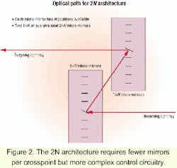
In the N2 approach, the position of the mirror is either on or off, and the specific light beam is directed by the mirrors that are held in the on position while all the others are in the off position. For the NxN switch, there are a total number of N2 micro-mirrors (see Figure 2). This approach requires a simple two-output-level driving circuit, with no special requirements for high voltage or linearity.
In the 2N architecture, each mirror is tilted to one of its N positions to reflect the light beam to the outgoing fiber. For each input fiber there is one micro-mirror, while each output fiber has its own micro-mirror. For the NxN switch, the total number of the micro-mirrors in the optical crosspoint is 2N. Some crosspoint implementations of the 2N architecture use a reflecting surface, allowing all of the micro-mirrors to be in one plane, thereby simplifying construction.The N2 approach is most useful for smaller optical crosspoint switches and has the advantage of simplified electronic control. However, as the number of crosspoints increases, the number of mirrors increases quadratically, making this approach uneconomical for large optical crosspoints. For large optical crosspoints-generally greater than 16x16-the 2N architecture offers better economy and performance. This approach does require more complex control circuitry to actuate the micro-mirror. Also, for 2N architectures that deploy electrostatic actuation, much higher voltages are necessary to position the mirrors.
The current state of the art in MEMS fabrication technology, combined with the properties of the optical signals, specifies a minimum mirror size and tilt angle for effective operation. These parameters, among others like the supporting flexures, dictate the required spacing between the plates that, in turn, dictates the voltage levels required for actuation. Today, typical 2N optical switches require operational voltages in the range of 150-250 V to achieve precise control for at least N different positions of the micro-mirror.
Previously, these high-voltage amplifiers were only available as discrete implementations, using high-voltage transistors combined with lower-voltage optical amplifiers. While early optical crosspoint switches were able to deploy these discrete drivers, their disadvantages moving forward are substantial. They include high cost, low accuracy, and increased board area with decreased functionality.
Integrated multichannel, high-voltage amplifiers are the natural solution to the driver requirements of the future-and this is an area where IC manufacturers are focusing. IC processes are now available that allow the combination of high voltage and precision control in one integrated circuit, thereby providing considerable advantages for future optical crosspoint switch designs.
There are several important attributes of integrated high-voltage amplifiers that are critical to their successful use in driving optical MEMS mirrors. Besides the high-voltage requirement, the amplifiers require good initial accuracy, as well as good DC performance over time and temperature. Because of the large number of high-voltage drivers used per switch, power consumption, integration of external components, and channel density are very important. While precision is most important, AC characteristics cannot be ignored, as there are minimum slew rate and bandwidth requirements that must be met. Additionally, programmable features, including current limiting and power shutdown, are often desirable.For high-voltage amplifiers, there are several parameters to address for maintaining acceptable accuracy. They include offset voltage, gain error, channel-to-channel matching, power supply rejection ratio, and common-mode rejection ratio (CMRR). In addition to these initial specifications, maintaining DC accuracy over temperature variations and over the lifetime of the equipment is also of critical importance.
For all MEMS-based optical crosspoints, there is an initial training procedure that the switch runs through to properly align each mirror to all of its possible N positions, with this information stored in memory. This process uses a complex algorithm that is time dependent on the initial accuracy of the electronic control components. For the high-voltage amplifiers, better initial accuracy translates to reduced training time. In large crosspoints, not all channels can be aligned properly due to failure of a specific MEMS mirror. For this reason, backup channels-comprising extra mirrors, amplifiers, or converters-are included in each switch to provide redundancy.Of equal importance is the change in DC characteristics over time and temperature. Offset voltage drift, gain temperature coefficient, and variations of offset and gain related to aging of the components need to be minimized for efficient switch operation. Excessive DC parametric shifts over time and temperature require more frequent retraining or re-calibration in the field, and may even cause some channels to become inoperative over time. Consequently, the high-voltage amplifier must be carefully designed to avoid these degradations.
Because of the large number of high-voltage amplifiers used per optical switch, characteristics that affect packing density are also important. Chief among these are the number of channels per package. Devices are available that offer 16 high-voltage amplifiers in a 64-lead package, providing adequate density for today's optical switches.
Additionally, since each switch re quires numerous amplifiers in a compact space, power dissipation must be minimized to prevent overheating, which could seriously degrade system performance. Including the gain-setting resistors on the chip provides two advantages. System density is improved, since each amplifier re quires two gain-setting resistors. So 32 external resistors are eliminated for a 16-channel amplifier, and the improved matching of the resistors available in an integrated circuit enhances the channel-to-channel gain match, improving system calibration and operation.Today, switching times for optical MEMS crosspoints are typically less than 5 msec, and most of this time is taken by the settling of the MEMS mirror, generally leaving less than 1 or 2 msec for the settling of the driver circuitry. This requirement places certain demands on the AC characteristics of the high-voltage amps. In particular, each amplifier must be able to slew on the order of 200 V and settle to 0.l% accuracy or better within 1 msec. Amplifier stability is also a consideration, as each MEMS mirror presents a capacitive load on the order of 150 pF to the amp, necessitating careful design to avoid oscillations.
Some features can be incorporated in high-voltage amps to enhance system performance and reliability. Power shutdown can be implemented by various design techniques to save system power.
For high-voltage amps employing operation al transconductance amplifier architectures, current-setting resistors can be programmed externally to maximize the power dissipation versus AC tradeoffs. Programmable gain, in ternal high-voltage switching capability, and internal electrostatic discharge (ESD) protection are other features providing benefits, depending on each MEMS switch design.
A combination of experienced analog design techniques and a state-of-the-art high-voltage process resulted in a 16-channel high-voltage amplifier that meets the requirements of the optical MEMS switches.
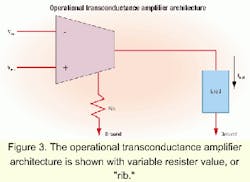
An architecture design used by some manufacturers is an operational transconductance am plifier (OTA) (see Figure 3). The pure capacitive load of some micro-mirrors makes them perfect for using an OTA design. The characteristic of an ideal OTA is nearly equivalent to that of the operation amplifier, except that the OTA has much higher output impedance. An OTA can achieve relatively small area with a good CMRR. Another benefit of OTA is its programmable biased current, called tail current. In such devices, variable value of a resistor called "rib" can be chosen to program the tail current. Proper selection of this resistor determines the tradeoff between power dissipation and AC performance.
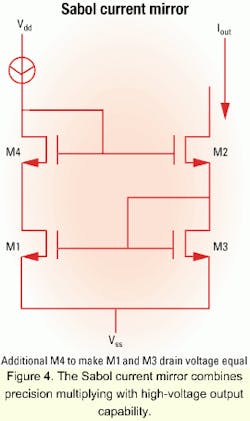
To achieve reduced power dissipation without sacrificing slew rate or limiting current, a precision current gain is accomplished by means of the Sabol current mirror (see Figure 4).Positive-channel metal-oxide semiconductor (PMOS) devices are used on the input stage to minimize bias currents. Diffusion metal-oxide semiconductors (DMOS) and high-voltage PMOS devices are used in the output stage to provide the high voltage drive for the micro-mirrors. Special ESD protection is also included. Besides the standard ESD protection on the pad, modified Wilson current sources are used to offer better ESD protection for the output stage.
The gain-setting resistors are internal to achieve the required matching to better than 2%. The feedback resistor comprises many unit resistors with each unit resistor matched to the input resistor. The non-inverting in put for all the amplifier channels is shared to save on pin count. All channels have the same fixed gain, with typical values between 32 and 40 depending on the particular mirror requirements.
For the high-voltage driver, like any successful IC circuit, careful layout is crucial to keep the system stable and functional. The matching metal-oxide semiconductor transistors should be in the same orientation and be as close as possible. Key transistors should be laid out with a common centroid geometry to improve matching of their threshold voltages, VT.
Careful circuit layout also helps to improve temperature stability. Sixteen feedback resistors, input resistors, and biased-current mirrors all have special matching requirements. The layout of the gain-setting resistors is especially important to minimize gain mismatches. High-power dissipation de vices, especially the high-voltage-output DMOS transistors, are distributed equally to minimize thermal gradients across the die.
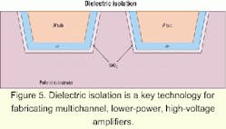
One particular process has a special answer to the high-voltage requirement-a 300-V power technology, fabricated on dielectrically isolated (DI) substrates. The component list includes a double-diffused N-channel DMOS for high-voltage/current switching, a high-voltage PMOS, diodes, bipolar transistors, a variety of capacitor and resistor configurations, low-voltage 20-MHz CMOS logic, and a family of zener diodes for protection and referencing. Design flexibility is achieved by offering low- and high-voltage device integration, with fully scalable devices based on circuit requirements.
The basic structure for the technology can be seen in Figure 5. The DI process is superior to p-n junction isolation because of its higher isolation voltage (1,000 V), smaller isolation area (BV>150 V), and noninterference between devices. Separate oxide-isolated silicon islands are supported by a poly-silicon handle, allowing complete isolation between low- and high-voltage devices. The DI isolation technique results in low parasitic capacitance, elimination of CMOS latch-up, and reduced power consumption.
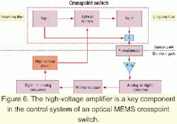
One typical application of high-voltage IC amplifiers in optical MEMS is the optical MEMS crosspoint switch. Figure 6 shows the O/E signal path in the optical crosspoints switch, with the upper part for the optical path and lower part for the electrical path.
In the optical path, the incoming light beam passes Tap 1 (an optical splitter), where a small amount of light (~1%) is split off and sent to the amplifier. The main beam is redirected by the micro-mirrors inside the optical crosspoint switch. After it has been redirected, it passes another tap, Tap 2, where a portion is split off and also sent to the amplifier. Separate amplifiers and detectors can be used, or the input/output can be selected by an optical switch, as shown in Figure 6.
The entire system is a closed feedback loop under the control of a microprocessor. The light split off from Tap 1 is transformed to an electrical signal by an optical PIN diode photodetector. Because there is a large variation in light level presented to the PIN diode, a wide dynamic range amplifier (transimpedance or log amp) is required to amplify the signal for the analog-to-digital (A/D) converter.
The A/D converter, usually on the order of 14-16 bits of resolution, converts the analog signal for the processor, which compares the two feedback signals from the input and output. The microprocessor makes the necessary adjustments to its output to minimize the optical signal attenuation for each crosspoint-switch setting. The processor output feeds a digital-to-analog (D/A) converter, which also is typically 14 to 16 bits of resolution.
The D/A converts the digital signal from the microprocessor to an analog signal capable of driving the input of the high-voltage amplifier. The high-voltage amp increases this low-level signal to the required high voltage to drive the mirror to the correct angle or tilt, as calculated by the system processor. Fine adjustments continue to be made to minimize the attenuation of the signal.
Automatic and periodic recalibration is a continuous process to maintain system performance over time and temperature changes.
Multichannel, high-voltage IC amplifiers provide performance improvements, increased density, and potential cost savings for MEMS applications versus the discrete implementations of the recent past. This trend of higher integration will certainly extend beyond just the high-voltage amplifiers.
Initially, over the next several years, further integration of the amplifiers and mixed-signal circuits will occur to minimize the space occupied by the control circuitry. Improved mixed-signal process technologies employing silicon-on-insulator (SOI) techniques will aid in this endeavor. Since the optical MEMS mirrors are processed using standard silicon fabrication methods, it is reasonable to assume that the control circuitry and micro-mirrors will eventually be integrated on the same piece of silicon, providing increased reliability, density, lower cost, and improved performance over time. SOI fabrication will likely be a major enabler for this integration as well.
Yuan Ma is an applications engineer for analog products and Ken Timko is a product-line manager for analog products at Agere Systems Inc. (Allentown, PA). They can be reached via the company's Website, www.agere.com.

