Modeling signal integrity in electro-optical systems
'Gray box' models and appropriate test and simulation tools can help designers predict the performance of electro- optic devices, including modulators and amplifiers.
JEFF MEYER, Cisco SystemsAccurate electro-optical-component models are a prerequisite for simulating the signal integrity of a high-speed optical-network line card. Most component vendors do not provide simulation models for their semiconductors or optical modules. Therefore, it is difficult to simulate the performance of the electro-optical system prior to fabrication.
In the analog and radio-frequency literature, there have been many references to "black box" modeling techniques.1 Black box modeling requires no understanding of the physics inside the component. Black box models must be generic, which often limits the level of nonlinearity in the component.
Another technique for modeling is known as "gray box" modeling, which is the process for deriving a model where something is known about the basic internal topology of the component but there are no detailed component values. In the case of optical modulators and modulator driver amplifiers, we have a basic understanding of the internal topology but no explicit model of the interconnect network and packaging. The topology of a photo-absorptive modulator consists of an interconnect network driving a PIN diode in parallel with a 50-ohm load resistor. The capacitance of the PIN diode and parasitic reactances of the interconnect network limit the overall performance of the modulator. Following is a process to derive the topology and values for such interconnect networks:
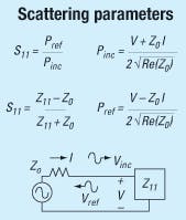
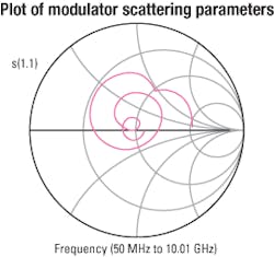
- Measure the scattering parameters (S-parameters) of the interconnect network in the frequency domain.
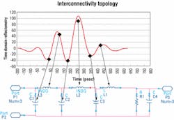
- Convert the frequency domain S-parameters into the time domain with time domain reflectometry (TDR) transform.
- Derive the topology of the interconnect network with the TDR response.
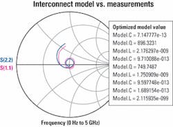
- Optimize the interconnect network model to match measured S-parameters in the frequency domain.
- Derive a gray box model for the nonlinear parts from measurement or data sheets.
- Combine models in a transient or harmonic balance simulation.
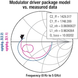
Once the topology is identified, circuit simulation software is used to optimize the lumped network component values for best match to measurement. The results of this optimized model compared to measurement are shown in Figure 4.
Electro-optical modulation curve
A model for the electrical-optical conversion of the PIN absorptive photodiode modulator must be derived by taking a simple measurement of optical attenuation versus DC modulator bias. The model for the attenuation versus bias can be created with a polynomial curve fit and modeled with the EDA (using the Symbolic Defined Device in the ADS 2001) or with a polynomial-dependent voltage source in SPICE. This dependent source derives its control voltage from the PIN diode monitor port on the interconnect network (see Figure 3). The modulator attenuation as a function of modulator bias is fit with a polynomial in the following equation:
p=12.54x+36.49x^2
+58.9x^3+36.98x^4
+10.16x^5+1.03x^6.
The complete model for the electro-absorptive modulator includes the interconnect network, followed by the polynomial dependent voltage source (curve-fitted to the modulation data).
Modulator driver modeling
The PIN absorptive photodiode modulator is driven from a 2.5-Gbit/sec square wave generated by the high-speed laser driver. A detailed SPICE model for the laser driver is also not readily available, but the semiconductor vendors provide a data sheet with an equivalent circuit for the high-speed driver amplifier.5 In this case, the equivalent circuit of the driver amplifier is a bipolar junction transistor (BJT) differential pair with a programmable current source.
The same S-parameter and TDR technique helps derive a lumped model for the laser modulator driver package. We can use this package model, together with ideal BJT model parameters, for the active devices.
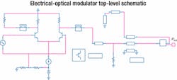
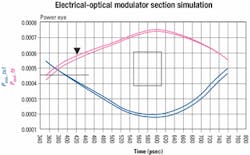
Simulating all the piecesAfter we have established a model for the package, we can model the entire system, which must also include the PC board interconnect network. In this case, the only PC board element is a quarter-inch length of 25-ohm microstrip transmission line and a pad for an optional shunt resistor.The electro-optical modulator model includes the conversion from electrical to optical power. The voltage output at the Pout node in Figure 6 should really be interpreted as power in milliwatts. Final simulation results of the modulator section are shown in Figure 7. For further confidence, we can simulate the optical power waveform as a function of time and compare it with measurements from a digital communications analyzer.
Achieving accurate simulation
For signal integrity analysis and modeling of a high-speed telecommunications network line card, an accurate simulation of the electro-optical system can be achieved with careful modeling of the electro-optical components in the frequency domain and time domain. Microwave S-parameter measurements and modeling techniques provide an accurate simulation model for the interconnect network of the photo-absorptive PIN diode modulator and modulator driver chip. Nonlinear effects such as the electro-absorptive PIN diode modulation curves can be measured and modeled with lookup tables or curve-fitting. The nonlinear driver amplifier can be modeled with the aid of the vendor application-note schematic.
Using these models, the system performance can be simulated with either a transient simulation or harmonic balance simulation. The results of the simulations are in good agreement with actual optical eye mask measurements.
Jeff Meyer is a technical leader in the optical ASIC engineering group at Cisco Systems (San Jose, CA).
References
- T.R. Turlington, Behavioral Modeling of Nonlinear RF and Microwave Devices, Artech House, ISBN 1580530141.
- "S-Parameter Design," Agilent Technologies Inc., Application note AN 154.
- "Time Domain Reflectometry Theory," Agilent Technologies Inc., Application note AN 1304-2.
- A.V. Oppenheim and R. Schafer, Digital Signal Processing, Prentice-Hall, 1975, ISBN 0132146355.
- "Advanced Design System 2001, Circuit Simulation Manual," Agilent Technologies Inc., August 2001.


