Long-wavelength VCSELs ready to benefit 40/100-GbE modules
By JEAN-CLAUDE CHARLIER and SVEN KRÜGER
Due to their inherent low cost, low power, and small size, 850-nm vertical cavity surface-emitting lasers (VCSELs) are currently being used in over 90 percent of Fibre Channel and Ethernet transceivers. By taking what was learned at 850 nm and extending it to 1310- and 1550-nm wavelengths, companies are now starting to show that they can drastically reduce the cost, power consumption, and size of long-wavelength transmitters.
Long-wavelength VCSELs come of age
Historically, VCSELs for longer wavelengths of 1300 to 1700 nm have been difficult to produce because of the refractive index of InGaAsP. But in the early 2000s, development of different combinations of III-V elements led to more practical long-wavelength VCSELs. At that time, several manufacturers such as Bandwidth9, Cielo Communications, E2O, and Picolight had proven that lasers supporting wavelengths higher than 980 nm were possible to produce in volume. However, after the explosion of the Internet bubble in 2000, none of those companies still exit, because they either didn't survive or were acquired.
Ten years later, work in long-wavelength VCSELs has revived with more mature technology mainly due to some new process technologies. Several companies, mainly in Europe, are now dedicated to long-wavelength VCSELs: Alight Technologies (Denmark), BeamExpress SA (a Swiss startup company spun off from the BeamExpress Inc. NeoPhotonics acquired in 2006), Vertilas GmbH (Germany), and RayCan (Korea).
The key advantages of VCSELs at shorter wavelengths remain at these longer wavelengths. They include the ability to be tested at the wafer level, which decreases processing costs and improves manufacturing yields significantly. VCSELs also enable easier coupling and packaging, thanks to their circular beam.
However, as need for speed continues to increase exponentially, the key advantage of VCSELs remains their very low power consumption as opposed to Fabry-Perot and distributed feedback (DFB) lasers.
This advantage is significant as requirements for data rates greater than 10 Gbps continue to emerge in both carrier and enterprise networks. The new 40-Gigabit Ethernet (GbE) and 100-GbE singlemode optical interfaces specified in the IEEE 802.3ba 2010 standard have become high priorities, yet present the greatest technological challenges when it comes to significant reductions in transceiver power dissipation and form factor. A 10X increase in speed implies a far greater increase in power consumption, which not only adds to the OEM's burden of removing excessive heat from systems, but is also diametrically opposed to the customer's desire for lower power operation.
Long-wavelength VCSELs therefore are now emerging as an attractive alternative to conventional lasers for these high-speed applications. However, the reliability of long-wavelength VCSELs has always been questioned by the industry because of the lack of solid supporting data. These questions may begin to disappear in the near future, as recently some long-wavelength VCSEL suppliers have started publishing solid reliability data on their devices.
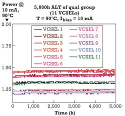
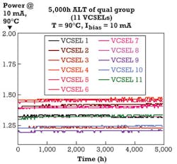
For example, long-wavelength VCSEL manufacturers have conducted extensive reliability testing in the last several years. High-temperature accelerated aging of 5,000 hours with zero failures and a mean time to failure (MTTF) value of >30 million hours at 25°C and about 2 million hours at 70°C have been published on 1310-nm waveband VCSELs created using wafer fusion (see Figure 1).
Wafer fusion (bonding) is a well-established process that provides very reliable and reproducible results. It is widely used in silicon technology for the production of silicon on insulator (SOI) structures and micro-electromechanical (MEMs) devices and also in GaAs technology (GaAs-based structures fused to GaP) for large-scale production of red light-emitting diodes (which, in fact, are similar to VCSELs in structure). GaAs-based to InP-based wafer fusion technology enables production of long-wavelength VCSELs delivering power in excess of 1 mW at temperatures above 70°C and at any wavelength from 1200 nm to 1650 nm.
VCSELs and 40G transceivers
VCSELs emitting in the 1270-1330-nm and 1500-1600-nm wavelength ranges are of increasing interest as alternatives to edge-emitting lasers because of their inherent low power consumption and high efficiency coupling into singlemode fiber. Together, these attributes enable significant reduction in transceiver power dissipation as well as form factor. These benefits are especially pertinent today as the industry struggles to reduce power dissipation and form factor for the next 40G and 100G optical interfaces using CWDM.
40GBase-LR4 (4x10-Gbps) optical transceivers in QSFP+ modules using uncooled DFB lasers are already on the market, with power dissipation specified at 3.5 W. However, new VCSEL-based transmit optical subassemblies (TOSAs) using low power consuming 10G VCSELs at 1270 nm, 1290 nm, 1310 nm, and 1330 nm have been recently demonstrated that can transmit data at 40 Gbps over 10 km. For next-generation 40GBase-LR4, the use of singlemode VCSELs and low power consuming VCSEL drivers will result in more than 40% power consumption savings, reducing 40-GbE optical transceiver power dissipation significantly below today's 3.5-W barrier.
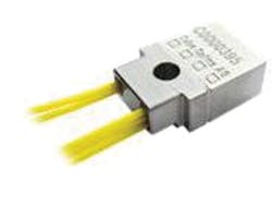
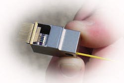
The appropriate package is a key factor to enable small, low-power QSFP+ devices using long-wavelength VCSELs (see Figure 2). This package not only demands high-efficiency optical coupling and RF design at the lowest cost points, but also needs to provide the yield and reliability rates necessary to support high-volume production.
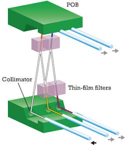
A technology that has proven its advantages in these terms is used to drive the optical engines of today's 40-Gbps and 100-Gbps LR4 CFP transceivers. These smaller passive CWDM and LAN WDM devices are based on a polymer optical bench (POB) structure (see Figure 3). The POB is a free-space optical design that relies on an injection-molded part that features high-precision alignment structures for the passive assembly of fibers and thin-film filters toward arrays of integrated collimators. Since the collimators are used in reflection, the beam path is polymer-free. This structure and the temperature change compensating design enable the device to exceed Telcordia and MIL standard reliability targets.
The next step in size reduction can only be achieved by removing the fibers from the transceiver to achieve a higher integration level. The POB technology not only enables the combination of passive optical elements but is also ideally suited to host active elements such as photodetectors or lasers - especially low heat dissipating VCSELs.
POB-based 40-Gbps and 100-Gbps receive optical subassemblies (ROSAs) that not only feature the optical demultiplexer with the integrated photodetectors but also the transimpedence amplifiers have been demonstrated over quite some time and are now entering the production stage. The same principles are used as well to couple and multiplex the four CWDM VCSELs to one output fiber-optical receptacle. Here as well the laser drivers are contained. To meet the QSFP+ performance, mechanical, and cost requirements, the ROSA and TOSA are best hosted in one housing that features both parts with a low-cost RF glass feed through interconnections to the transceiver board (see Figure 4).
Thanks to the combination of energy-efficient VCSELs and low-loss free-space optics (FSO) multiplexing, the use of high-density packages with power dissipation of <2 W might become achievable in the not so distant future, permitting unprecedented high port density at the system level.
VCSELs and 100 GbE
Initial implementation of 100-Gbps modules will incorporate the rather bulky CFP transceiver package, but a smaller form factor clearly would be preferred. System makers seek power consumption reduction of more than 50%, which will ease system thermal management and enable 100-GbE port count scaling. The use of 10 edge-emitting lasers in a small-form-factor package, however, creates serious thermal management concerns. By contrast, long-wavelength VCSELs are well positioned to address a new 100G MSA, as they would enable a drastic reduction in overall power consumption and the use of high-density packaging.
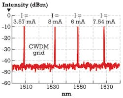
First prototypes of such a high-density CWDM TOSA using four VCSELs at four different wavelengths near 1.5 μm have been demonstrated (see Figure 5). The VCSELs were multiplexed into singlemode fiber using a low-loss FSO multiplexer, and the device was measured to have an emission spectrum compatible with the CWDM grid (see Figure 6).
In summary, wafer-fusion technology is inherently well designed for the fabrication of multi-wavelength VCSEL devices with high-precision wavelength settings. The solid long-term reliability results these devices show should assure the industry that long-wavelength VCSELs are now ready for incorporation into optical communications equipment.
JEAN-CLAUDE CHARLIER is CEO at BeamExpress SA. SVEN KRÜGER is vice president, product management at Cube Optics.
