Quantum dot lasers and silicon photonics advance data-center connectivity
New pathways to low power and cost will open the door to more efficient data-center network architectures.
The insatiable demand for "smart devices" with faster connectivity coupled with cloud as a means of storage and computing resources has revolutionized the fabric of data centers in recent years. They have led to the emergence of a new architecture focused on faster, more resilient content delivery networks.
This new architecture evolution in data centers has resulted in a growth industry that's showing no signs of abating. Expenditures on data-center systems, including servers, Ethernet switches, and storage, were estimated to be over $147 billion in 2013, with a growth rate of 4.5% year over year.1 This spending trend will continue as the need to deliver a "better user experience" drives increased investment in new disruptive technologies. These new technologies will also enable a scalable and cost-effective network infrastructure for cloud, mobile, social, and big data/analytics.
One key area of focus in recent years has been on new optical technologies that reduce interface cost while supporting longer reaches at increased data rates for both 2-km intra-data-center connectivity and 100-km inter-data-center superchannel connectivity.
Changes in data-center architecture
According to a study conducted by Cisco Systems, data-center traffic on a global scale will continue to grow at a 25% compound annual growth rate (CAGR), with the fastest growing segment being the cloud data-center traffic at 35% CAGR, a 4.5-fold growth from 2012 to 2017.2
To further corroborate the changes inside the data center, Cisco's 2013 Global Cloud Index report suggests that data-center traffic will triple by 2017 and a staggering 76% of that traffic is within the data center's server-to-server traffic. This important trend in data-center networking is driving requirements for denser server connectivity and longer network reach.
Unfortunately, a simple scaling based on current optical-interface technology within the data center contradicts the requirement for reduced network complexity and fails to deliver a cost-effective approach. Data-center operators will require much higher density optical interfaces that offer scalability from tens or hundreds of gigabits to terabits per second.
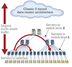
Data-center networks have traditionally been designed to support conventionally managed hosting services, where the majority of the data flows in and out of the data center based on traditional north--south traffic flow in a three-tiered hierarchical design (see Figure 1).3 But hierarchical data-center networks have grown complex, power hungry, and costly in terms of optical-fiber use and optical interfaces. This approach is ill-suited for the machine-to-machine traffic required of today's growing services and evolving applications.
In addition, server-to-server traffic in a three-tiered architecture increases network latency when traffic traverses multiple network layers in a north--south direction. This three-tiered architecture doesn't fit with today's widespread adoption of server virtualization and distributed computing that drives an increasingly "east--west" traffic plan.
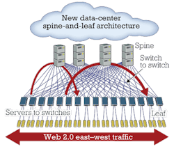
As such, moving to a two-tiered spine-and-leaf architecture enables the data-center operator to address today's changing traffic patterns and effectively eliminate the aggregation layer from the previous design (see Figure 2).4 Furthermore, this architecture provides a lower latency solution and is better suited to accommodate high bandwidth and delay-sensitive inter/intra-data-center traffic flows.
Enabling a better approach
To maximize the advantages that the new generation of spine-and-leaf architectures offer, as well as open the door to eventual use of superchannel connectivity, a new generation of optical interconnectivity is required. This technology must:
- Satisfy the increasing demand for bandwidth.
- Deliver significant reduction in the power dissipation, size, and cost of optical interconnects.
- Reduce network latency.
An extremely promising approach toward meeting these requirements pairs innovation in quantum dot multiwavelength (QD MW) lasers with advanced digital and photonic integrated-circuit technologies.
A QD MW laser is a nano-crystal semiconductor device capable of generating multiple wavelengths simultaneously. A single QD MW laser can provide up to 96 wavelengths in the C-band alone, which would enable the replacement of 96 individual lasers in an equivalent system. The overall gain bandwidth of the QD MW laser is over 90 nm, which enables future scalability for up to 200 wavelengths.
The QD MW laser enables a much simpler and more compact interface design, resulting in lower power consumption and better performance when compared to an equivalent design with multiple discrete lasers and components.
Meanwhile, photonic integration has become a key area of research and development in recent years for optical-network equipment vendors wanting to reduce the cost and size of optical interfaces. Silicon technology and integration enables system vendors to replace expensive optical components with their silicon counterparts such as modulators, multiplexers/demultiplexers, filters, attenuators, switches, and detectors.
A novel use of silicon photonics has resulted in the implementation of optical modulation on a micro-ring resonator architecture that enables high-speed modulation at data rates up to 56 Gbps. These ring modulators act like a wavelength-sensitive switch. When the ring is not in resonance, the optical signal passes straight through with minimal loss. Conversely, when the ring is resonant, the optical signal is coupled into the ring and no longer passed through.
These modulators are fabricated with a silicon-on-insulator process using silicon waveguides that provide natural vertical and lateral confinement via a ridge. Such ring resonators are ideal WDM building blocks and can be cascaded to construct WDM transceivers. In such a construct, each ring provides a multiplexing, demultiplexing, and modulation operation in a geometry that's well suited to extreme scaling of many channels.
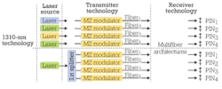
When we couple a single QD MW laser source, which generates multiple wavelengths simultaneously, with a silicon photonics ring architecture, we get a 1550-nm design that greatly reduces the overall cost and networking complexity within the data-center optical interconnect (see Figure 3).
In contrast, Figure 4 illustrates how existing transceiver architectures using traditional 850/1310-nm single-wavelength laser technologies are ideally suited to multifiber designs that fail to cost-effectively scale to higher capacities primarily due to the required fiber plant complexity.
To cost-effectively scale data-center networks to meet growing data rates, operators must future-proof today's infrastructure investment.
Network economics
A study that compared a Parallel Single Mode, 4 Lanes (PSM4) approach against the QD MW/silicon photonics design described earlier shows a significant advantage for 1550-nm designs with single-fiber connectivity as opposed to multiple fiber strands. The study estimates a 2.5X to 4X cost advantage when using the single-fiber approach as capacity scales from 100G to 1.6T for intra-data-center links.
Another study looked at inter-data-center connectivity with links of up to 120 km. The study compared the basic transmitter layout of coherent architectures for 100G and 400G to the one based on the QD MW laser with silicon photonics ring resonators. The study demonstrated over 5X power reduction and 24X size reduction using the latter approach when compared to coherent 400G architectures. An evaluation of the full link cost for scaling the 400G link for 120 km for data-center interconnect based on both the coherent and QM MW/silicon photonics approaches showed a 2X to 3X cost advantage for the non-coherent design.
These studies demonstrate that the combination of the QD MW laser and silicon photonics devices is an ideal implementation for inter/intra-data-center interconnects. These technologies have demonstrated a significant cost and power advantage relative to discrete implementation and enable a much higher scalability for the next generation of data-center infrastructure.
References
1. Gartner report, May 2013.
2. Cisco Global Cloud Index: Forecast and Methodology, 2012--2017.
3./4. James Kisner, "Technology -- Silicon Photonics: Data Center Disruptor," Jeffries, 2/22/13.
SAEID ARAMIDEH is the chief marketing and sales officer for RANOVUS Inc., a startup focused on next generation interconnects for the telecom and information technology industries.
Archived Lightwave Issues


