By Matt Traverso
Overview
The conventional approach to transmitter and receiver design, in which each element comes in a discrete package, will not prove beneficial for 100-Gbps DWDM. At least some aspects of photonic integration will need to be applied.
To address the growing need for 100-Gbps DWDM optical interfaces, the Optical Internetworking Forum (OIF) has begun development of Implementation Agreements (IAs) for optical transmitters and receivers. Historically, such optical transmitter and receiver multi-source agreements (MSAs) or IAs have been strictly confined to simple optical-to-electrical (OE) or electrical-to-optical (EO) converters. Some examples include the XMD MSA for 10-Gbps optical subassemblies, as well as the follow-on XLMD MSA for 40-Gbps optical subassemblies. These MSAs could specify simple OE/EO conversion because the modulation scheme for encoding the data was on (1) and off (0) keying using amplitude modulation.
However, for 100-Gbps DWDM, the OIF has focused on a modulation scheme known as dual-polarization quadrature phase-shift keying (DP-QPSK) paired with coherent detection. This modulation scheme requires more complex optics to transmit and receive the data. The application of photonic integration to these optics promises optimized designs.
Motivation for DP-QPSK for 100-Gbps DWDM
The DP-QPSK modulation scheme is attractive for next-generation speeds such as 100 Gbps due to its lower symbol rate. The impairments in an optical fiber link scale relative to the symbol rate of the signal. For example, chromatic dispersion of the optical fiber causes the optical spectrum of a pulse to spread, with the redder portion of the pulse travelling more slowly than the bluer segment. So for a given length of optical fiber, the spectrum spreading affects higher-speed transmission more strongly because the bit times are much shorter. Thus, a lower symbol rate reduces the impact of this chromatic dispersion.
Additionally, a key motivation for a lower symbol rate is spectral efficiency. Large DWDM-based networks often transport as many wavelengths as possible over a single fiber to achieve a spectrally efficient use of the fiber bandwidth. The common wavelength spacing in long-haul networks today is 50 GHz, with various filters such as reconfigurable optical add/drop multiplexers (ROADMs) or wavelength multiplexer/demultiplexers truncating each 50-GHz channel. This truncated spectrum places an upper limit on the symbol rate. Thus, for use in established fiber-optic networks, it is necessary to select a 100-Gbps modulation scheme with a lower symbol rate.
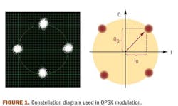
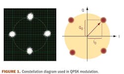
The DP-QPSK modulation scheme reduces the symbol rate relative to a 100-Gbps bit rate in two fundamental ways (Figure 1). First, the signal is split into two polarization states, allowing the required symbol rate to be divided in half. Second, the signal is phase modulated with two bits per symbol, again dividing the required symbol rate in half. This yields a symbol rate of a nominal 25 Gbps, which is much more robust in the face of link impairments than a 100-Gbps symbol rate would be. (It should be noted that this article uses nominal data rates of 100 Gbps and 25 Gbps. However, actual rates in operation will be higher to accommodate OTN mapping as well as the overhead for forward error correction encoding.)
The focus on DP-QPSK also has an advantage beyond a lower symbol rate. For 10-Gbps data rates and below (where the symbol rate and bit rate are identical), simple OE/EO converters for amplitude modulation are used across the board. Beginning at 40 Gbps, however, various companies have deployed at least four different modulation schemes. This proliferation of modulation schemes has fragmented the 40G optical networking market with customized optical transmitters, customized optical receivers, and unique digital ICs designed for each. The result has been generally higher technology costs.
This and other drawbacks of a multitude of customized 40G products motivated the optical networking industry to focus resources on common modulation schemes such as DP-QPSK and associated building blocks for 100-Gbps DWDM to leverage greater economies of scale.
Optical transmitter and receiver overview
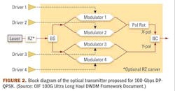
The OIF’s 100-Gbps optical transmitter is the Integrated Polarization Multiplexed Quadrature (PM-Q) Modulator as shown in Figure 2. There are two basic sections to the transmitter structure: the polarization segment and the QPSK modulator section. The splitting of the two polarization states is determined by the polarization rotator, as well as the optical characteristics of the waveguides. As shown in the diagram, modulators 1 and 2 form a single QPSK modulator for the X polarization, while modulators 3 and 4 form a single QPSK modulator for the Y polarization.
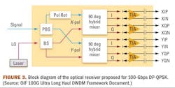
The 100-Gbps optical receiver being defined by the OIF is the Integrated Dual Polarization Intradyne Coherent Receiver (Figure 3). There are three sections to the optical receiver as defined in the IA: the polarization segment, the optical mixer section, and the high-speed detector section. The polarization segment must be composed of polarization-maintaining waveguides with both a very good polarization beam splitter and polarization rotator. The 90° hybrid mixers are dependent upon good optical coupling and the polarization characteristics of the preceding elements. Finally, as in 10-Gbps and lower receivers, the high-speed photodetector and transimpedance amplifiers must have high bandwidth and gain with low noise characteristics.
Photonic integration
Both the DP-QPSK optical transmitter and receiver require multiple elements to support their operation. The optical transmitter has polarization elements and modulation elements, while the receiver must support polarization elements, as well as optical mixing elements and high-speed photodetectors and electronics.
The conventional design approach would be to construct each of these elements in discrete packages, with the goal of optimized performance for each element. The implementation challenges with such a strategy are threefold: the complexity of the interconnections, the resulting overall size, and the different materials typically used for each element.
Photonic integration of the optical transmitter and the optical receiver addresses at least some of these challenges. Photonic integration solves the challenge of interconnect complexity by placing many of the most parameter-sensitive interconnects into the hands of a single designer. A conventional discrete implementation of the DP-QPSK optical receiver would require up to five interconnects with controlled polarization fiber. This discrete architecture would lead to manufacturing challenges, as well as complication of the characterization and specification tradeoffs of the various discrete elements.
Implementing a transmitter or receiver design via photonic integration affords great advantages in module size. In conventional discrete designs, each component is burdened with a hermetic standalone package that must be individually mounted to the system board. These package outlines obviously extend the system size. However, the biggest size penalty arises from the shaping and routing of the fiber and electrical interconnects.
As mentioned earlier, optical interconnects are hampered by the fiber routing, as well as the requirements regarding polarization control. The electrical interconnects are similarly constrained both in size and difficulty by the strict skew budgets and high baud rates of the individual data lanes. A package based on photonic integration solves most of these size constraints.
However, one challenge with photonic integration is the incorporation of disparate material systems into a single package. For example, MZI modulators are often constructed using lithium niobate (LiNbO3), while the lasers used for DWDM systems are constructed from indium phosphide (InP)-based semiconductors. Unfortunately, these two material systems do not coexist well in a single package; cross contamination between the two materials will occur, which results in device failure. To address any material compatibility issues, therefore, the OIF has architected the optical transmitter and receiver to combine functions that typically use complementary materials.
The OIF IA for the optical transmitter and optical receiver includes a mechanical envelope and electrical interface for each. This approach creates a system where the designer can be somewhat agnostic as to the specific technologies and materials used in the construction of the transmitter and receiver. This design paradigm is ideal for photonic integration as it allows the designer and manufacturer of the optical transmitter or receiver to use the technical and material approach best suited for their technology and manufacturing processes.
We can expect that these OIF-based IAs will aid in the deployment of 100-Gbps DWDM systems. The use of photonic integration will drive a more robust supply chain for high-speed optics while leveraging the technologies developed for 40-Gbps systems.
Matt Traverso is director, strategic marketing, at Opnext (www.opnext.com).
Links to more information
Lightwave e-Conference: Optical Internetworking Forum’s 100G Activities
Lightwave Online: OIF Issues 100G Framework Document
Lightwave Online: The OIF Defines 100G Project for Module Mangement Interface


