By Dr. Matt Pearson
Overview
Planar lightwave circuit (PLC) technology, originally developed for low-cost optical access products, is now being applied to other markets, including advanced 40G/100G applications.
The development of planar lightwave circuits (PLCs) has focused mainly over the last few years on fiber-to-the-home (FTTH) applications, where small size and low cost are paramount. PLCs collapsed many optical elements onto a single optical chip; manufactured using processes comparable to those used in the fabrication of electronic integrated circuits, PLCs enabled designs very well suited for FTTH.
PLCs continue to play an important role in the FTTH market today. However, they have evolved significantly and, in some cases, now offer functionality that is often unachievable in micro-optic assemblies.
For example, the interest in advanced 40G/100G networks has grown dramatically, and this presents a new opportunity for the use of PLCs. In a significant departure from the FTTH application, in which PLCs are valued mainly for their low-cost, high-volume manufacturability, these new 40G/100G applications look to PLCs to deliver optical functionality that is not readily achievable using traditional bulk optics.
A means to an end
There are typically two ways to support 100G links: through the use of DWDM or through advanced modulation formats like differential quadrature phase-shift keying (DQPSK) and polarization-multiplexed quadrature phase-shift keying (PM-QPSK). These advanced modulation formats have revolutionized the way networks are designed, but present a number of challenges to system designers and optical component manufacturers.
DQPSK and similar technologies offer a means of transmitting 40G and even 100G optical signals along optical fiber, most of which was designed to support 10G traffic. To enable this performance, DQPSK, QPSK, and similar formats use phase modulation as a means of encoding data at extremely high bit rates. Optical demodulators decode these signals at the receiving end.
Very precise phase delays and other subtle optical effects are used at each end of the 40G/100G optical link. Some of these effects can be extremely hard to control in traditional fiber-based optical components. Even relatively simple tasks, like splicing and connectorizing fibers, become complicated in these systems.
For example, the 90° optical hybrid demodulator in a PM-QPSK receiver can include eight separate fibers, each coupled to its own detector. To control phases in such a receiver, it is necessary to splice or connectorize each fiber in a way that all fibers exiting the mixer are equal in length, with millimeter-scale precision. That means that if seven fibers are successfully completed and then the eighth fiber gets damaged and needs to be re-cleaved, the seven other splices must be broken and re-cleaved to match the new, shorter length. This complicates assembly and has a significant impact on yields and even the viability of this approach for large-scale deployment.
PLCs have a clear advantage in this application, since the waveguides that route light inside an optical chip are lithographically defined. This means that physical path lengths on the PLC can be controlled with nanometer precision.
In addition to lithographically defined phase delays, PLCs also provide a means to integrate thermo-optic phase shifters throughout the optical chip. This enables active phase control that can be adjusted as necessary and monitored in real time. This has proven to be a valuable building block for advanced 40G/100G components.
PLCs and integration
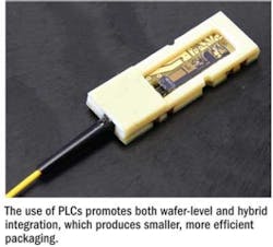
In addition to the phase shifting elements and other optical functionality embedded in the PLC itself, there is an equally important need for integrating active components with the PLC. These active components include things like lasers and photodetectors, along with transimpedance amplifiers and other electronic circuitry. In most cases, these active components are integrated to the PLC through hybrid integration techniques, which enables PLC designers to use the best possible active components for their application, without compromising performance by trying to fabricate everything on a single wafer. This strategy also simplifies PLC processing; the use of multiple vendors helps minimize risk and lower costs through competition, as well.
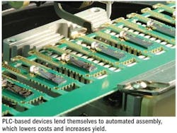
A wide array of PLC technology platforms were developed to address the low-cost, high-volume FTTH market, and that development continues today. However, it is clear that the most successful PLC platforms to date leverage passive hybrid integration methods that do not require the lasers or detectors to be powered up and monitored during high-volume assembly. Such active alignment is much more complex and requires significantly more time and expense in assembly.
Passive integration of subcomponents onto a PLC platform has evolved dramatically over the past 5 to 10 years. At one time, it was considered nearly impossible to bond photodetectors to a PLC in a repeatable, high-volume assembly process. But more recent developments in PLC wafer fabrication, automated alignment systems, and component design have revolutionized the way optical components are manufactured. In addition to photodetectors, it is now also possible to align and bond high-performance lasers that require nearly 10X the alignment accuracy of a photodetector, using processes capable of producing tens of thousands of units per month or more.
The ability to passively integrate diode lasers to a PLC platform is a result of several innovations in wafer processing and optical design. In the past, only custom lasers were compatible with most PLC hybrid integration processes. This limited the number of vendors, and thereby affected the cost of these lasers. Recent advances have shown that standard diode lasers of virtually any type can be integrated onto a PLC platform through passive alignment. This approach uses a multi-core waveguide platform, in which light from hybrid lasers mounted on top of the PLC is collected by a series of specially formed waveguides, then coupled to more typical waveguide structures buried well below the surface of the chip.
A primary focus during this development was on reducing back reflections within the PLC structure. As a result, nearly any type of laser can now be integrated with the PLC, even those that are highly sensitive to back reflections. Distributed feedback (DFB) lasers, and even new externally modulated lasers (EMLs), can potentially be bonded in very high volume processes. This achievement represents a significant advancement in the manufacture of long-haul optical components for 40G/100G networks.
Most laser diodes used in telecommunications rely on thermal tuning to ensure the laser wavelength remains in the correct location on the ITU grid. In a bulk-optic approach, this tuning is normally accomplished by packaging every laser in its own package that includes a thermo-electric heater/cooler to maintain the proper temperature.
In PLCs, we often want to add significantly more functionality into a much smaller package, and it is not uncommon for a single PLC chip to contain 4, 8, 12, or even more lasers. Each laser still must be thermally tuned to the correct grid wavelength, and it is impossible to accomplish that with a single large heater/cooler under the PLC substrate. Instead, the same technology used to manufacture thermo-optic phase shifters in PLCs can now be leveraged to make miniature heater elements on the surface of the PLC.
These small, localized heating elements can be included under each hybrid laser, and are all individually addressable, allowing each laser to be thermally tuned to the ITU grid. This is but one example that demonstrates how PLCs incorporate not just optical elements, but also thermal, mechanical, and electrical elements, as well.
At the opposite end of the link, high-speed photodetectors can be bonded directly to the PLC surface, creating receiver modules ideally suited for high-bandwidth 40G/100G applications. While waveguide-based photodetectors can be used if needed, standard surface-illuminated photodetectors sometimes offer more simplicity, lower cost, and, in some cases, even higher performance. To couple light from the PLC waveguide to the surface-mounted photodetector, it is necessary to bounce the light 90° from horizontal to vertical. This is accomplished through on-chip mirrors fabricated in the PLC itself as part of the wafer manufacturing process.
Like their electronic counterparts, PLCs can be designed with impedance-matched electrical traces, which are used to interface detectors with TIAs and package feedthroughs. This approach provides the most optimal high-bandwidth electrical performance available, clearly an important consideration for 40G/100G components running at extremely high data rates.
PLCs have, at times, been mistakenly viewed as nothing more than a means to manufacturing low-cost optics. In actuality, PLCs now offer performance that is sometimes not viable in bulk-optic assemblies, and integrate thermal, mechanical, and electrical innovations, in addition to the underlying optics.
As 40G/100G network requirements continue to evolve, so will the demands for increased functionality from optical components. PLCs provide a clear path for integrating that functionality onto a single PLC platform that is suitable for high-volume assembly.
Dr. Matt Pearson is vice president, technology, at Enablence Technologies Inc.
Links to more information
Lightwave: Photonic Integration Diverges down Two Paths
Lightwave: 100G Challenges Equipment Design
Lightwave Online: Systems Vendors See No Time to Wait for 100 Gbps


