By Jon Anderson
With the first generation of modules beginning to ship, work is already underway to reduce transceiver power and form factor.
With the recent completion of 40G/100 Gigabit Ethernet (GbE) optical interface standards (IEEE 802.3ba-2010) and pluggable optical transceiver module specifications (CFP-MSA Rev 1.4), and with the production shipment of first-generation 40GbE/100GbE CFP products underway, optical module vendors are now focusing on developing technologies and proving design-ins for their next-generation 40/100GbE pluggable optical transceivers. Key objectives include significant reductions in module power dissipation and size, which are critical to increasing system port density and reducing overall optical port cost for system vendors and their customers.
The 100GbE CFP module provides the highest faceplate density (in terms of Gbps per faceplate aperature-module pitch area) for MSA-specified pluggable optical modules to date. However, from a systems point of view, the CFP port density most likely will be limited by thermal constraints on power dissipation, which may typically be greater than 25 W for first-generation 100GbE CFP modules. This article discusses some of the key challenges facing optical module vendors considering these design objectives and outlines some of the more promising technical approaches to tackle and overcome these challenges.
First-generation 40/100GbE pluggble optical transceivers
Let's first review the technologies and designs of choice in the first generation of 40GbE/100GbE pluggable optical transceivers. The 40GbE and 100GbE optical interfaces specified in IEEE 802.3ba-2010 are summarized in Table 1.
From a market application perspective, the 40GbE and 100GbE LR4 singlemode fiber optical interfaces are high priority and present the greatest technological challenges when it comes to significant reductions in transceiver power dissipation and form factor size.
CFP 40GBase-LR4 design. The first-generation 40GBase-LR4 optical transceiver is based on a 4x10G architecture that comprises the following discrete components:
- 10G CWDM 1310-nm uncooled directly modulated distributed feedback (DM-DFB) transmit optical subassemblies (TOSAs)
- 10G PIN photodiode (PD) with integrated transimpedance amplifier (TIA)
- receive optical subassemblies (ROSAs)
- four-channel optical multiplexing/de-multiplexing filters
- quad dual-channel clock/data recovery (CDR) IC. The quad CDR IC provides the XLAUI 4x10G electrical interface defined in the IEEE Std 802.3ba-2010 specification.
These components are packaged into the pluggable CFP module; the module's mechanical, electrical, and management interface specifications are given in the recently completed CFP MSA Rev. 1.4, as shown in Figure 1. The CFP module-host system management interface is based on the IEEE Std MDIO/MDC interface and includes several new features, such as programmable controls and alarms, module state transitions, and error rate calculations. The first-generation design leverages existing 10G optoelectronic device technology and uses innovations in packaging to realize high-performance, low-cost modules for high-volume production.
The CFP 40GBase-LR4 module power dissipation is typically in the range of 6 W, which fits well within the CFP module's 32-W power maximum. Thus, there is considerable interest in reducing the 40G-LR4 module form factor in next-generation designs for increased 40GbE port density. This will be addressed later in this article.
CFP 100GBase-LR4/ER4 design. The first-generation 100GBase-LR4/ER4 optical transceiver architecture is similar to that of the 40GBase-LR4, but with the speed of the active optoelectronic components increased to 28 Gbps for realizing a 4x28G optical interface. Additionally, the CAUI electrical interface defined in IEEE 802.3ba-2010 is widened from 4x10G lanes to 10x10G lanes. A 10:4/4:10 "gearbox" serializer/deserializer IC is used to implement the electrical interface between the 10-lane host data path and the four-lane optical data path.
The optical interface defined in IEEE 802.3ba-2010 uses a four-wavelength LAN-WDM 800-GHz wavelength grid in the 1310-nm band and optical multiplexing/de-multiplexing on singlemode fiber. The transmitter optical specifications for LR4 and ER4 are based on cooled electro-absorption modulation with integrated DFB (EA-DFB) laser technology, but were written to allow eventual implementation with directly modulated DFB lasers for smaller size, lower power consumption, and lower cost TOSAs.
The receiver optical specifications for LR4 and ER4 are based upon PIN-PD detector technology with integrated TIA. The receiver specification also includes optical amplification, such as from a semiconductor optical amplifier, to compensate for optical fiber attenuation loss in the ER4 40-km application.
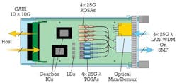
These components are packaged into the CFP pluggable module (previously shown in Figure 1) with non-coaxial, 28-Gbps electrical connections between the discrete component TOSAs, ROSAs, and gearbox IC, as illustrated in Figure 2.
The first-generation 100GBase-LR4 module power dissipation is typically in the range of 24 W, which poses significant thermal management challenges for system designers, particularly as they seek to increase 100GbE optical port density. Thus, there is strong motivation to significantly reduce the 100GBase-LR4 optical transceiver module power dissipation in the next-generation design.
Next-generation 40GbE/100GbE optical module design targets
For the next-generation 40GbE/ 100GbE optical transceiver modules, system designers want significant reductions in power dissipation and form factor size. These objectives are particularly critical as system houses work to scale their core switching and routing input/output capacities and reduce constraints on port densities due to thermal management limits.
For 40GBase-LR4, the priority target is module form factor reduction. In terms of faceplate density, the current CFP form factor for 40GbE ports is 2.5X less efficient compared to the 100GbE CFP.
One approach the CFP design enables is to double or possibly triple the number of 40GbE ports within a single CFP module. While this approach increases port density, it suffers from reduced port provisioning modularity.
A more feasible approach is to make use of the existing QSFP+ form factor (SFF-8436) and the non-retimed XLPPI electrical interface specified in IEEE 802.3ba-2010. This approach increases faceplate density by more than 60 percent over the CFP while retaining port modularity. To make this switch, however, optical module vendors need to not only reduce the physical size of their optical components, but they must reduce component power dissipation by over 50 percent so as to fit into the 3.5-W maximum power envelope of the QSFP+.
For 100GBase-LR4/ER4, the priority target is power dissipation reduction. System makers are looking for power consumption reduction on the order of 50 percent or more. This will ease system thermal management and enable 100GbE port count scaling in the short term. For the longer term, however, system designers seek 100GbE transceiver roadmaps with significant reductions in both power dissipation and form factor size.
Next-generation 40GbE/100GbE technologies
Several promising technological advances in progress could be used by optical module designers to achieve their next-gen 40GbE/100GbE module design targets. These include:
- laser array/planar lightwave circuitry (PLC) hybrid integrated TOSA
- PD/TIA array/PLC hybrid integrated ROSA
- low-power BiCMOS ICs and CMOS gearbox IC
- Narrow 4x28G-VSR electrical interface, electrical connector, and 28G CDR IC
- CFP2 electro-mechanical module development.
Hybrid integration of DFB discrete or array lasers with optical multiplexing PLCs has been investigated intensively across the industry. Some of the key challenges to using this technology in TOSA development include laser/PLC device alignment and optical coupling loss minimization. Use of a laser array is desired, as it minimizes the number of process steps in active alignment with the PLC device. However, a DFB laser array is particularly challenging to realize with sufficient gain across all channels for a wide temperature range. Nevertheless, four-channel devices appear to be feasible for realizing an optical hybrid integrated TOSA.
Similarly, hybrid integration of PIN-PD and TIA arrays with optical de-multiplexing PLC has also been investigated. Early progress using this type of ROSA was made with 10GBase-LX4 module designs, so it appears feasible to scale ROSA rates up to 4x10G and 4x28G. Challenges still remain in PD/PLC device passive alignment, control of attenuation and polarization mode dispersion losses, and temperature stability for realizing an optical hybrid integrated ROSA.
Significant reduction of 40GbE/ 100GbE optical transceiver power dissipation will come from improvements in the component ICs. For next-generation 40GBase-LR4, use of the non-retimed XLPPI electrical interface enables elimination of the quad CDR device, which results in more than 30 percent power consumption savings. Further process and design improvements in laser drivers and TIAs will assist with an overall module power consumption reduction of over 50 percent.
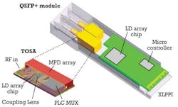
Figure 3. Next-generation 40GBase-LR4 optical transceiver design.
For next-gen 100GBase-LR4, EA-DFB driver IC process improvement and CMOS gearbox ICs will be a major factor in module power consumption reduction. With these factors, plus improvements in TIA and module DC-DC power conversion, 50 percent overall CFP module power dissipation looks feasible in the near term.
For the longer term, it is desirable to narrow the module electrical interface to four parallel lanes operating each at 28 Gbps. This would enable replacement of the gearbox IC with a quad 28G CDR IC, thus reducing electrical interface IC complexity and power consumption. Work is underway in the Optical Internetworking Forum (OIF) to specify a host chip to optical module electrical interface, called CEI 28G-VSR. Electrical connector suppliers, physical layer IC suppliers, host system vendors, and module vendors are working together in the OIF to confirm application requirements and specify a 28G channel model and electrical interface characteristics.
Even with all of these developments, it still appears that 100GBase-LR4 power dissipation will be on the order of 10 W, which is still too high to fit into the existing QSFP+ form factor power envelope. To reduce module form factor size, consideration of a next-generation CFP module, "CFP2," is underway that would be compactly sized for sub-10-W power dissipation and support a narrow 4x28G electrical interface.
With the above-noted technology advances, the next-generation 40GBase-LR4 QSFP+ conceptually could be realized as illustrated in Figure 3. A future 100GBase-LR4 CFP2 would look similar architecturally, with operation at 4 x28G and inclusion of a quad 28G CDR electrical interface. The CFP2 module dimension specifications are an open point of study at this time, but past design experience suggests the CFP2 may look mechanically similar to the existing X2 form factor.
Future trends
First-generation 40GbE/100GbE CFP optical transceivers are now completing customer qualification and shipping in production. Key design targets for next-generation optical transceivers are: significant reduction of module power dissipation and form factor size.
Critical technologies for tackling these design targets include 4x10G and 4x28G hybrid integrated TOSAs/ROSAs and process improvements in 28G gearbox and CDR ICs. There also may be consideration of uncooled CWDM 28G laser technology for realizing 100GbE optical transceivers in a QSFP+-like form factor for short singlemode fiber (<2 km) applications.
Table 1. IEEE Std 802.3ba-2010 optical interfaces.
Physical Medium | 40GbE | 100GbE |
Multimode Fiber (at least 100 m OM3) | 40GBase-SR4 | 100GBase-SR10 |
Singlemode Fiber (at least 10 km) | 40GBase-LR4 | 100GBase-LR4 |
Singlemode Fiber (at least 40 km) | Not Defined | 100GBase-ER4 |
Jon Anderson, Ph.D., is director of technology programs at Opnext.
Past LW Issues


