by Pierluigi Franco, Marco Romagnoli, and Francesco Tassone
In the market for optical transceivers for WDM applications, pluggability and tunability hold the key to achieving cost reductions in transport optical equipment. Equipment suppliers have been highly successful in developing a variety of technologies that provide either tunable or pluggable devices, but combining both tunability and pluggability in one module�without increasing the overall size�has proved to be a much more difficult challenge. Few suppliers have been able to demonstrate a combined tunable and pluggable product within the size of a standard XFP module and, although the first tunable DWDM XFP for 10-Gbit/sec applications was launched in March 2007, commercial introduction of such modules is not expected much before the end of 2008.This article examines the main drivers in creating the need for tunability and pluggability and the advantages of combining both features into one optical device along with the different technological approaches used to combine the two features.
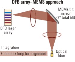
Tunability has been one of the strongest drivers in the telecommunications market in recent years. Tunable lasers have many advantages, not least of which is enabling a reduction of inventories and, therefore, capex and opex costs in WDM transmission systems. Today transmitter tunability is a fundamental requirement in reconfigurable optical networks, especially in combination with other optically tunable elements such as tunable or reconfigurable add/drop multiplexers.There are three main technological approaches used in the implementation of tunable lasers. The most established one leverages a widespread WDM laser technology to combine up to 12 distributed feedback lasers (DFBs) with evenly spaced emission wavelengths into a single chip array.1 The output of the 12 lasers is then selected using a MEMS-based turning mirror (Fig. 1). Fine tuning is achieved by thermal tuning of the DFB of up to 3 nm. The existence of moving parts in the form of MEMS, however, may affect the long-term reliability of this approach.
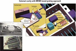
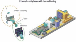
The second technology uses external-cavity semiconductor lasers, again well established on the laboratory bench scale. This technology, however, requires the development of ultrasmall mirrors to fit into small packages. Such reductions have been achieved in three main ways: either by using MEMS-based turning mirrors2 to the external grating (Fig. 2) or via either of two approaches that do not rely on moving parts, which makes them more reliable. These two are based either on tuning the grating reflectivity using a liquid-crystal layer or on thermal tuning of silicon-based etalons (Fig. 34).
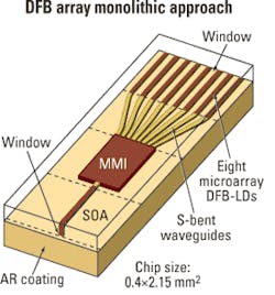
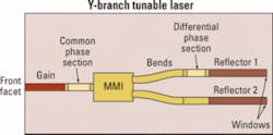
Given the size limitations of these approaches, a monolithic approach is desirable to reduce the size of the tunable laser. A first monolithic approach is based on the DFB array,5 where the laser outputs are combined into a single output by a lossy MMI multiplexer (Fig. 4). Large loss at the MMI is compensated by an integrated amplifier at the chip output.A second monolithic approach relies on the integration of the external tunable mirrors,6�8 as shown in Figs. 5 and 6. In both cases the whole tunable laser is manufactured as a single InP chip just a few millimeters long and less than 1 mm wide. Moreover, the ability to integrate external modulators on the same chip has already been demonstrated, potentially leading to a very compact modulated laser source. A different monolithic approach to the tunable mirror was also demonstrated previously.8
However, these monolithic approaches are all based on a major technological advance that is not as well established on an industrial mass production level as the standard DFB technology. It consists of the integration onto the same substrate of active gain waveguides with passive waveguides where tunable reflectors and/or well balanced MMI splitters are realized. A reasonably high yield is then required to demonstrate the potential low cost expected of this approach. Several suppliers have been able to show the feasibility of the monolithic approach on a large scale, though it remains to be seen whether the yield problems can be solved.
In practice, tunable laser sources are all currently packaged in relatively large butterfly packages used in combination with standard LiNbO3 modulators with standard MSA 300-pin modules. LiNbO3 modulators are a technological standard, unsurpassed at the performance level, but rather bulky and expensive. At the same time, more compact and cheaper InP-based modulators are becoming interesting in emerging lower-end applications, albeit with an inferior performance.
The alternative to tunability in recent years has been the development�largely driven by datacom applications�of pluggable optical modules, with form factors such as SFP, XFP, X2, XENPAK, etc. The two most successful form factors in telecom optical systems have been the XFP and SFP, used primarily in 10- and 2.5-Gbit/sec applications. Their success is based on the need to build single-standard-compliant transmission cards using different optical pluggable modules depending on the required application. These carry the performing functions and are thus more expensive than transmission cards, moving the inventory problem from the card to the pluggable optics level.The table summarizes the current situation.
The next natural step in the evolution of transmission interfaces for 10-Gbit/sec DWDM systems is the combination of tunability and pluggability in the same device, bringing together the inventory advantages of each approach. There are, however, significant technological challenges, especially with the need to maintain the same footprint for combined modules.
The most suitable format for a tunable-pluggable transceiver for 10-Gbit/sec DWDM applications is the XFP. The smaller SFP, even in the slightly larger SFP+ format, is currently considered still too small for these applications. Both the tunable laser source and the 10-Gbit/sec high-performance modulation function then need to be squeezed into a tunable optical subassembly (TOSA) of much smaller size than butterfly packages. Some vendors have produced larger modules, but there is very little enthusiasm within the industry for such devices.
The technological challenges vary according to which tunability approach (see Fig. 1 through 4) has been adopted. The size of the standard DFB array plus MEMS turning mirror approach in Fig. 1 is some tens of millimeters long, due to the limited turning angle of the MEMS mirror and the required spacing of DFBs in the array chip to allow for connections. The coupling optics to an external wideband modulator also has to be added. Unless major advances in MEMS technology are implemented, it is difficult to see how this approach can be squeezed into a standard TOSA that measures 1 to 2 cm long.
Direct modulation of the DFB chips looks even more challenging, as a 10-Gbit/sec electrical switch and appropriate RF connections to the array would have to be implemented. Concerning direct modulation, the same can be said of the DFB array approach seen in Fig. 4.External-cavity lasers are also relatively long. In the approach shown in Fig. 3, tuning is based on two etalons plus a thick phase section on the external mirror, making it difficult to reduce the physical size of the laser. However, an approach has been developed where the physical length of the cavity can in principle be squeezed to just 2 to 3 mm by appropriate development of compact intracavity coupling optics. In this case, the space remaining within a 1-cm TOSA package could be sufficient for coupling to a compact InP-based external modulator.
On the other hand, all the monolithic approaches to tunable lasers�with their short lengths�are well positioned to integrate low-performance external modulators either at a hybrid or monolithic level. The monolithic integration of the external modulation looks more attractive, since in this case the resulting chip will fit into a small TOSA package.
However, the further integration of at least another passive and active amplification section in the device means that substantially lower yields are to be expected compared to the already presumably low yields of the tunable laser section. Moreover, the requirement of relatively large injection currents in the three gain sections (cavity, laser amplifier, modulator amplifier) in order to recover sufficient output power�both for the hybrid and monolithic approaches�could become a serious issue for electrical power requirements and thermal dissipation in the XFP approach.
Chirp management of DS-DBR, SSG-DBR, or Y-branch tunable lasers seems challenging considering the extensive cavity lengths required for the tunable reflectors, a fact that presumably reduces chirp far below manageable levels. Instead, a further squeezing of external cavity approaches to the millimeter level would allow a chirp-managed approach to work, thus avoiding the requirement of an external modulator with its amplification section.
The best approach appears to be hybrid integration using a silicon-on-insulator (SOI) waveguide platform. This provides a technically feasible method to achieve advantageous tuning capability (demonstrated over several tens of nanometers with less than 100 mW of heating power) and sub decibel/centimeter losses that are suitable for integration of further optical functionality at the laser output. The hybrid integration approach allows the best use of both technologies, while avoiding their major drawbacks: lack of light generation and amplification for silicon, and reduced yields/high costs and increased power consumption when integration of passive functions such as tunable mirrors and optical filters are required in the III-V device. Since the SOI device fabrication process runs on 8-inch wafers, the small devices required in the tunable sources become relatively inexpensive. This therefore clearly demonstrates the advantages of this technology in terms of performance, cost, and power requirements.
Considering the current stages of development in the tunable/pluggable scenario, several predictions can be made for the development of DWDM optical interfaces over the next 3 to 5 years.
First, in terms of form factor, all of the 2.5-Gbit/sec applications will migrate to the SFP format, with 10-Gbit/sec applications moving to XFP format and 40+ Gbit/sec applications moving to the MSA 300-pin format. Tunability will be available in XFP and MSA 300-pin formats, but not for the SFP (even though the larger SFP+ format could host tunability at 2.5 Gbits/sec). And finally, as regards the modulation format, direct modulation will be the reference technology for 2.5 Gbits/sec and for low-end 10 Gbits/sec, with chirp management technique being a good candidate for high-end 10-Gbit/sec transmission. At 40 Gbits/sec and above, LiNbO3 will remain the reference modulation technology.
Pierluigi Franco is senior vice president, Technology Department, within the Photonics Business Unit of Pirelli Broadband Solutions (www.pirelli.com). Marco Romagnoli is vice president and chief scientist, optical design and characterization, and Francesco Tassone is scientist, advanced laser source development, at Pirelli Labs.
- B. Pezeshki et al., Proc. OFC, Paper ThGG71, 2002.
- D. Anton et al., �Mode-hop Free Sweep Tuning of a MEMS-tuned External Cavity Semiconductor Laser,� Proc. CLEO, 2004.
- K. Sato et al., J. Lightwave Technol., Vol. 25, No. 8, pp. 2226-2232, 2007.
- Intel Technol. Journal, Vol. 8, Issue 2, pp. 105-112, 2004.
- H. Hatakeyama et al., �Wavelength-selectable Microarray Light Sources for S-, C-, and L-Bands in WDM Applications,� Proc. OFC, 2004.
- L.A. Coldren, IEEE J. Selected Topics in Quantum Electron., Vol. 6, No. 6, pp. 988�999, 2000.
- D.J. Robbins et al., �A High Power, Broadband Tunable Laser Module Based on a DS-DBR Laser with Integrated SOA,� Proc. OFC, 2004.
- J.-O. Wesström et al., Proc. OFC, Paper TuE2, 2004.
- Y. Matsui et al., IEEE Photon. Technol. Lett., Vol. 18, No. 2, pp. 385�387, 2006.
