Solving the four Ps for future optical modules
The issues of performance, power, packaging, and price need to be resolved, as the addition of optical requirements to high-speed electronic requirements forces the use of new technologies.
DR. R.E. REEDY, Peregrine Semiconductor Corp.
Fiber-optic communication is used in both telecommunications and data communications. In general, a telecom application is a long-haul system utilizing singlemode fibers, DWDM, and 1.3- or 1.5-micron wavelength light. The light sources for telecom are typically expensive edge-emitting lasers, and modulation is usually performed with electro-optic modulators. Volume is relatively low (thousands or tens of thousands of pieces is a large order) and prices are relatively high.
The datacom market is different on virtually all these points: multimode fibers are combined with directly modulated vertical-cavity surface-emitting lasers (VCSELs) for transmission at 850 nm. Volumes are high (hundreds of thousands are typical volumes), and prices are often 10-100 times less per channel.
The telecom market is, of course, the backbone of the Internet, while datacom applications include storage-area networks (SANs), optical backplanes, and LANs. Although the focus here is on the impact of components and assembly techniques on the high-volume datacom market, many of the basic concepts apply to the telecom market, although key differences will be highlighted.
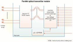
The optical module shown in Figure 1 is the type being considered here. A parallel array of multimode fibers is aligned and connected to an electrical package, which contains the electronic functions necessary to convert the optical signals to/from electrical signals. Current modules, such as those described in the Optical Internetworking Forum Very Short Reach specification or in the multisource agreement, are available on the Web.Currently, these modules are shipping from Infineon, Agilent, and others at volumes of hundreds of thousands of units per year, with forecasts showing they will increase to millions per year by the middle of this decade. As the cost per module decreases and functionality per module increases, more applications will be able to use the benefits of optical-fiber data transmission. However, it will be necessary for the new modules to show higher performance, lower power consumption, integration of more functions into a single package, and lower cost per function.
Performance. For optical interconnect systems in the datacom market, performance is set primarily by two parameters: data rate and jitter. Due to the distances involved, data rates in the telecom market have increased from 155 Mbits/sec (OC-3) through 622 Mbits/sec (OC-12), 2.5 Gbits/sec (OC-48), and 10 Gbits/sec (OC-192). Datacom applications could use conventional coaxial cable for short distances at the slower data rates (up to 622 Mbits/sec), so they did not need fiber-optic interconnects until the channel bandwidths approach 1 Gbit/sec. With the enormous increase in data bandwidth in storage systems and inside routers and switches, fiber-based communications became necessary. Again thanks to the shorter distances, multimode fiber could be used, which enabled the lower price point necessary for the higher-volume applications.The other key performance parameter is jitter, which is a form of noise. Optical systems transmit data by sending a train of light pulses down a fiber. The signal is degraded in both amplitude and timing by electronic circuits, optical devices, and the fiber itself. In multimode-fiber systems, the light pulses are dispersed at different velocities in each optical mode, causing the equivalent of an optical echo. By the time the light pulses reach the photodetector at the fiber's end, the light beam can spread substantially, encroaching on adjacent optical pulses. This so-called modal dispersion limits the distance that any given pulse of light can travel without creating intersymbol interference. Electronics and packaging (crosstalk) at both the receiving and transmitting end must be designed to add a minimal amount of jitter to the signal so the pulse transmission distance down the fiber can be maximized. (Crosstalk can only increase jitter, so crosstalk must be minimized.)
Power. Most high-performance electronic systems are operated at their power dissipation limit for a very simple reason: If more current can be applied, the system will go faster, but if the cooling limit is exceeded, system reliability will degrade to the point of failure.
For optical systems this issue is exacerbated by temperature sensitivity as well as the reliability of most lasers. For datacom systems, the VCSELs provide both low cost and low operating power, with high-performance lasers available with threshold currents below 1 mA and modulation currents to hit multigigabit-per-second performance well below 10 mA. With such low-power-consumption lasers available, it is critical to deliver the high-speed laser drive currents and photodetector amplification at very low power.However, laser drive currents and electronic I/O specifications often limit the degrees of freedom that designers can consider. Electrical I/O standards such as current mode logic or low-voltage differential signal often consume 50% to 75% of the total power budget in an optical module. So to reduce power, it is important to consider solutions such as lower rail voltages and increase functional integration. The latter is particularly valuable: By merging two chips into one chip (say a transimpedance amplifier chip with a clock/data recover chip) the output buffer of the first chip and the input buffer of the second chip can be eliminated, thereby saving 30% to 50% of the total power. Just as microprocessors reduced the power consumption of computers, integration of optoelectronic devices offers a path to reducing power consumption in fiber-optic modules.
Packaging. Packaging affects both performance and power consumption. At multigigabit-per-second data rates, inductance and capacitance of the package and bond wires have several troublesome effects. They can behave as a narrowband L-C filter, which would cause pattern-sensitive bit-error-rate issues. Bond wires and pack age parasitic capacitances often have Q-factors greater than 50, meaning the resultant filter effect can be quite narrowband, an effect that must be compensated for in some way.
The better approach is to ensure the package parasitics are small enough that the filtering effect is above the highest frequency of interest, commonly called "out-of-band." As data rates of 10 Gbits/sec be come common, this solution requires extremely low parasitics. For example, a 1-nH inductance (typical for a short bond) wire and a 1-pF capacitance (also typical for a bonding pad or package) has a resonant notch filter frequency of approximately 4 GHz, well within the 10-Gbit/sec signal.
Package components can also limit isolation between channels. Most commercial packages are limited to 30-dB isolation between adjacent channels. If there are resonances, or many channels, the total crosstalk can easily degrade the data signal. As modules move from 1x12 to 2x12 and beyond, and as data rates increase, packaging crosstalk issues will become increasingly difficult, thereby forcing extremely low parasitic packaging solutions such as flip-chip attachment.
Improvements in packaging techniques must also en able higher levels of integration. The primary driver for in creased integration is ease of use by the customer. Handling multi gigabit-per-second signals at the board level can be very difficult, even for engineers with high-speed experience. Many router, switch, and SAN companies, however, specialize in the large digital chips and associated software, finding the high-speed analog signals to be very difficult and risky. Integrating multiple high-speed functions into a single package offers such vendors reduced time-to-market; reduced risk; smaller board area; and lower power consumption.
Price. Product price is primarily driven by process complexity, yield, and volume. Of course, yield is often set by process complexity, with the number of critical steps in the exponent of most yield equations. For traditional optical modules, assembly and packaging can represent up to 50% of module costs. And since assembly yield losses occur late in the overall manufacturing process, yield loss at this stage substantially increases cost.
Increasing unit volume is the most straightforward way to reduce cost for two main reasons: Fixed costs are amortized over the larger volume, and higher volume creates a return on investment that supports the up-front costs of a yield improvement effort. So the lowest-priced solution will minimize the total process complexity (including device fabrication and package assembly and test), offers inherently high yield, and relies on components and process techniques already in high-volume production.
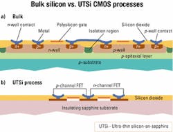
A new monolithic structure based on use of high-speed silicon CMOS fabricated on a transparent sapphire substrate, satisfies the four Ps (see Figure 2). The technology, called ultra-thin silicon-on-sapphire (UTSi) CMOS, produces a starting structure extremely well suited to optical communication functions.
Because of the insulating sapphire substrate and elimination of the substrate's parasitic effects, the UTSi process produces high-performance CMOS circuitry requiring less power than bulk silicon CMOS. In the current 0.5-micron UTSi process, modulation rates greater than 5 GHz are achievable. UTSi CMOS with 0.25-micron features will be available in 2001, allowing greater than 10-GHz modulation rates.Additional advantages of UTSi CMOS are the availability of multithreshold transistors and integrated EEPROM devices (i.e., non-volatile memory). Even with these enhancements, standard design and fabrication semiconductor tools are used. The fabrication process yield is comparable to bulk silicon, and processed wafer cost is much less than competing high-performance technologies such as GaAs, BiCMOS, or SiGe (none of which offer transparent substrates and the FOCUTS packaging option discussed below). The process is fully commercialized, with greater than one million components shipping monthly to commercial customers.
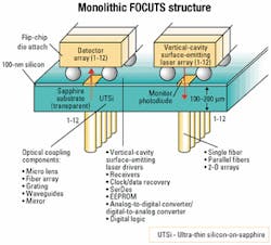
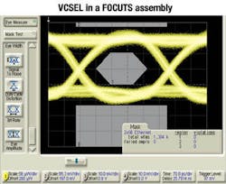
Fabricating high-speed, low-power CMOS circuits on a sapphire substrate allows for flip-chip bonding of optoelectronic devices onto CMOS circuitry to build flipped optical chip on UTSi (FOCUTS) modules (see Figure 3). Flip-chip bonding eliminates the wire-bond inductance between driving/receiving circuits and the optoelectronic devices, which becomes problematic at data rates greater than 2.5 Gbits/sec.* Flip-chip bonding also reduces the number of discrete chips that must be handled, packaged, and aligned in the final module, thereby reducing manufacturing costs.Figure 4 shows measured detected laser output from a flip-chip FOCUTS module (see Figure 3). The trace shows an excellent eye-diagram and low jitter. Power consumption for the laser driver and laser was less than 25 mW. The results were obtained from 0.5-micron UTSi CMOS. Future versions will include power monitor photodiodes and EEPROM trimming capability.
The assembly shown in Figure 3 will be delivered to the market in module form (see Figure 5). Inside this surface-mount package are the VCSEL drivers with VCSEL flip-chip attached and monitor photodiodes providing feedback control on all laser outputs. The entire module is expected to operate at 2.5 Gbits/sec and consume less than 100 mW per channel. Future versions based on 0.25-micron UTSi CMOS will increase the data rate and further lower power consumption.
Optical modules must simultaneously address performance, power, packaging, and price requirements if they are to enter high-volume markets. The FOCUTS concept addresses these issues in the following manner:
- Performance. Low substrate parasitics enable high-speed, low-power, and low-jitter circuits. Also, virtual elimination of packaging parasitics (bond wires and package capacitance) reduces bit-error rate and improves jitter on the transmitter and improves gain, stability, and jitter on the receiver. The sapphire substrate and low parasitics also improve isolation between functions and between channels, thereby reducing noise and jitter.
- Power. CMOS consumes the least power of any technology available but normally cannot hit the speeds needed by optical systems. UTSi CMOS hits the necessary speeds while retaining the fundamental power savings of CMOS. Also, reduced package parasitics provides additional power savings by eliminating the power used to drive the parasitics. And integration opportunities created by the monolithic assembly and ideal isolation will further reduce power consumption by reducing the number of power-hungry chip-to-chip interconnections.
- Packaging. The 12-channel monolithic structure shown in Figure 3 is approximately 4x2 mm, since fiber arrays are built on 0.25-mm fiber-to-fiber spacing. Integration of additional functions will further reduce total board area. And assembly costs are minimized by relying on CMOS fabrication techniques such as building in the monitor photodiode, rather than purchasing, aligning, and assembling this device afterward. As speeds increase to 10 Gbits/sec, elimination of the narrowband filtering effect of package parasitics will further increase the attractiveness of the FOCUTS technique.
- Price. CMOS is also the lowest-cost integrated-circuit technology available, thanks largely to the huge volumes over which all tools are amortized. Although UTSi CMOS requires a sapphire substrate, reduced processing and packaging costs more than offset this single (and relatively minor) expense. Furthermore, inclusion of EEPROM on the UTSi chip enables substantial yield enhancement at the final stages of assembly.
VCSEL or alignment variations can be measured at test and corrective values stored permanently in the EEPROM. The integrated monitor photodiode also can be used for temperature adjustment, end-of-life notification, or eye-safety monitoring, all of which are potential cost savings to the user.
Relying on a unique combination of high-speed electrical properties and near-ideal optical properties, UTSi CMOS on sapphire has been shown to offer new options to the development of optical modules. Integration of multiple functions and large arrays of devices will enable substantial improvements in speed, power, board area, and price.
Ashok V. Krishnamoorthy and Keith W. Goossen, "Optoelectronic-VLSI: Photonics Integrated with VLSI Circuits," IEEE JSTQE, 4(6) (1998).
Dr. R.E. Reedy is a co-founder of Peregrine Semiconductor (San Diego) and chief technical officer. He can be reached at [email protected].
