Lifting the lid off component integration
ICs revolutionized the chip industry, but optical ICs are creating opportunities for design improvement at each new level of complexity.
DAVID GAHAN, Bookham TechnologyHeated debate about integration in the optical-components industry continues, despite the technology advancements in recent years. Many companies argue that integration is the way forward. Integration, after all, was the path chosen by the microelectronics industry from the 1970s onward. Some companies still believe that integrated devices are more trouble than they're worth.
The prime motivation for integration is cost reduction. Integration is also the result of many forces within the market, which now requires component suppliers to provide subsystem levels of integration. Systems suppliers need integrated subsystems so they can focus on areas of value-add and differentiation rather than the nuts and bolts of a system that "merely works." These companies also need to meet exacting time-to-market specifications (notwithstanding current market conditions). The complexity of both system design and implementation is radically reduced by access to configurable, reliable subsystem-level components.
Integrated components also save space, which is of prime concern to network operators trying to squeeze extra return from their investment in facilities. Finally, and most important, systems built using integrated components exhibit better reliability and hence provide lower cost of ownership, a major factor in today's competitive market.
Silicon as an integration platform
The current debate among the integration supporters is over which technologies offer the best platforms. Silica has been the historical favorite of the components industry. Silicon, despite its standing as a widely understood material, had few advocates. The dynamics in the industry have changed, however. First, there has been growth in the number of companies using silicon as an integration platform. Second, real action has finally supplemented "talk" since truly integrated components (based on silicon technology) have entered the market.
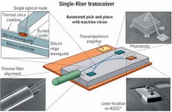
This process started with relatively simple components. The first integrated devices based on silicon that were produced in volume-single-fiber transceivers-began shipping in 1998. These devices, which are now deployed in hundreds of thousands of fiber-to-the-x systems, demonstrated the potential of silicon for component integration.
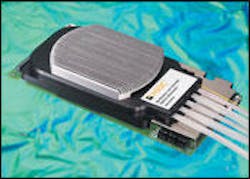
The next level of silicon integration followed soon after: Optical-channel-monitor devices combined photodetection and arrayed-waveguide-grating (AWG) functions. Multiplexers with variable optical attenuators (mux-VOAs) integrate the functions of AWGs with solid-state, charge-injection, controlled attenuators (see Photo). Both of these integrated components are now in volume production.The latest integration involves more complex subsystems such as optical spectrum analysis modules (OSAMs) with switching inputs. These devices, designed for next-generation long-haul transmission systems, are in the evaluation stage at customer sites.
Although the question of whether integration is "a good thing" is essentially answered, how this integration is accomplished is still widely debated. Many components suppliers now bundle several discrete or ganged devices into a single package, which they hope will pass muster with their customers. Unfortunately, this approach misses out on some of the key advantages of genuine integration. The production process for a multichip optical package is difficult to automate, which affects not only the cost of production, but also leads to inconsistencies in device characteristics when produced in volume. Internal fiber interconnects merely replicate ones normally found outside the package, and without true integration, miniaturization is restricted. Moreover, in fiber-interconnect designs, the individual packaging of key components effectively dictates the design and size of the overall package, leading to inflexibility in the current design and future development.
Platform characteristics
What attributes determine the success of an integration platform? The four major attributes are functionality, performance, ease of customization, and yield of the integrated circuits.
Functionality is the ability of the chosen platform to perform all-or at least most-of the tasks, both active and passive, required by engineers working in optical networking. These functions can be implemented intrinsically by building structures within the material of the optical device or by hybridization (i.e., attaching discrete devices directly to the surface of the optical substrate). Note that this approach is not strictly monolithic because of the presence of hybrid components. The substrate is not simply an interconnect; it also must offer the ability to implement a range of intrinsic functions, with hybridization used only where it is appropriate. By definition, unless the platform supports a range of functions, it is not possible to produce integrated components.
Integrated components must reach and eventually exceed the appropriate performance benchmarks of the industry. These components must perform not just as discrete components, but also when combined into a fully featured subsystem. It is relatively easy to implement the majority of optical functions using a range of technologies, but the art is to deliver the required performance when these functions are implemented in combination on the same substrate.Customization is required because customers are increasingly asking for fast, reliable production of a number of product variants. Here, the silicon approach provides a full set of optical functions easily integrated onto a single device and promises rapid turnaround. Because custom solutions generally provide lower-volume opportunities than off-the-shelf solutions, they traditionally fit well in the domain of hand-built integrated products, but this approach scales poorly as volume increases and is costly, time-consuming, and finding little to commend it, particularly in current market conditions.
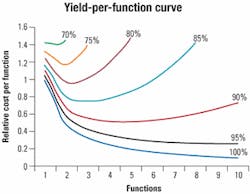
Manufacturing yield is another key parameter. Not only are well-understood, high-yield processes likely to be more commercially viable for cost reasons, but they also produce components that are less likely to fail in the field. The yield-per-function curve is an exacting one-for functional yields of less than 85% or 90%, it is more costly to produce an integrated component than several discrete devices (see Figure 1).
Switching elements
One of the keys to the functionality questions raised is about the availability of a reliable switching element that can be integrated with other standard components. Requirements and applications vary; therefore, a strong integration platform will allow switching to be implemented in different ways.
There are four basic factors to consider when assessing switch technologies. First, is it a "good" switch-does it perform in terms of switching speed, polarization dependence, signal blocking, and so on? Second, is it manufacturable? Third, can it be integrated? And fourth, how much does the technology cost?
Almost any component can be regarded as a switch, if it is deployed correctly and the surrounding components are integrated properly. The fast switching speed and high extinction ratio of a silicon-based electronic variable optical attenuator (EVOA) can be used to enable switching functions in many applications. The EVOA is a powerful building block within many subsystem-level products.
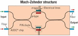
A solid-state EVOA uses carrier injection to achieve attenuation due to free carrier absorption within a silicon substrate. Carrier injection into the waveguide region is achieved using a PIN-diode structure (see Figure 2). Such a structure allows both electrons and holes to be injected in equal proportions. This physical mechanism of attenuation means that the switching speed of the device is approximately three orders of magnitude faster (~2 MHz) than thermo-optic devices. Attenuation is high (up to 60 dB), enabling the use of the EVOA for blocking applications and making the device an effective 1x1 switch.The use of a bipolar p- and n-type structure provides an efficient method of carrier injection; the level of injection achieved is orders of magnitude greater than that of unipolar devices such as resistors. The result is a device with an almost linear current/attenuation characteristic that is extremely fast, making it suitable for fast switching applications such as protection switching. The component can also be produced at yields high enough to justify integration. Polarization-dependent loss as an integrated component is virtually nonexistent and, in contrast to some alternative implementations, it is independent of attenuation.
The EVOA has been proven effective in several integrated components. One of the more noteworthy is a mux-VOA device that combines 80 optical functions on a single chip. This device is a good example of an important design consideration when integrating-that of thermal management. Almost all optical materials exhibit some degree of thermal sensitivity. Many technologies rely on thermo-optic effects to produce useful circuits, and silicon is no exception. AWGs are typically among the more thermally sensitive components, while current-controlled EVOAs generate heat-conflicting attributes in integrated devices.This problem can be efficiently managed in a number of ways. First, silicon is intrinsically thermally conductive, so it is relatively easy to remove excess heat from critical areas of the device. Second, the monolithic nature of the device enables engineers to design an overall package that fits in with thermal and performance requirements. Moreover, the EVOA structure is intrinsically a diode. It therefore stands to benefit from the continuous improvements in the microelectronics industry to minimize the power dissipated within the attenuators.
For higher orders of switching (2x2 and above), alternative structures can be more suitable. One implementation is a Mach-Zehnder (MZ) switch, typically consisting of two 3-dB couplers connected by two waveguides that serve as phase-shifters (see Figure 3). When light is launched into one of the two input ports, it is split into two MZ arms by the first 3-dB coupler. The two signals in the MZ arms have equal optical power and can be phase-shifted by changing the carrier concentration with a PIN-diode arrangement on either arm. At the second coupler, the two beams recombine constructively or destructively at either of the two output ports, depending on the exact phase difference between the two MZ arms. The accumulated phase difference can be modulated. Hence, for the purpose of switching light, the desired output can be chosen from the two output ports.This device, of course, depends on the use of electro-optic effects for its operation. It cannot be realized in non-electro-optic materials such as silica. A similar effect can be produced in such materials by replacing the PIN diode with a thermo-optic device, although these devices require higher power levels to reach equivalent extinction ratios.
Although the couplers attempt to divide the optical power equally, power imbalances can occur, reducing the achievable extinction ratio-in such a case, it is possible to use MZ switches in cascade format to increase the extinction ratio or deploy EVOAs to improve moderate isolation of the output signal. The cascaded MZ format also points to one way of achieving higher-order (NxN) switches in planar devices.
Monitoring and control
While switching is probably the most important single function currently under scrutiny in the integrated-component arena, monitoring and control represent the most critical system-level requirement for device makers. This requirement evolved over a number of years.
The early single-fiber transceivers used a simple tap and monitor structure to monitor a single channel via a photodiode (see Figure 4). That was followed by an integrated optical-channel monitor, which used AWG and PIN array technologies to isolate and monitor 40 DWDM channels.
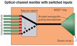
The next step is an optical-channel monitor with switched input (see Figure 5). This subsystem integrates an eight-way EVOA-based switch, a 60-channel demultiplexer, and 60 detectors into an optical processing device capable of monitoring over 400 independent channels.
Such monitoring strategies are essential as the momentum toward all-optical networking continues. Integrated components will look in creasingly like optical signal processors. And investment will increase in areas such as signal analysis and software algorithms. The debate over integration already has been won.
David Gahan is director of DWDM products at Bookham Technology (Abingdon, Oxfordshire, UK).
* ASOC is Bookham's proprietary design and manufacturing technology.
