Plasma-activated process key for low-cost Ethernet
The market for 10-Gigabit Ethernet in premises networks is now gaining traction and growing rapidly. The key technical enablers that have extended low-cost Ethernet to 10 Gbits/sec are short-wavelength VCSELs and ultra-high-bandwidth multimode fiber (MMF) with low differential mode delay (DMD) values and flat DMD profiles.
Until recently, the North American premises market almost exclusively used 62.5-µm MMF with bandwidth of 160 or 200/500 MHz•km. This fiber can transmit 10 Gbits/sec for only 33 m using conventional serial transceivers. By contrast, 50-µm fiber, with an effective modal bandwidth of 2,000 MHz•km at 850 nm, can transmit 10 Gbits/sec over 300 m. Largely for this reason, 2004 saw dramatic growth in the deployment of 50-µm MMF types that support 1- and 10-Gbit/sec applications. Industry data indicates that more than 30% of the quarterly shipments of MMF are these high-performance 50-µm fibers. According to KMI Research, demand for these fiber types will continue to grow and are forecast to reach 58% of the North American market and 70% of the Western European market by 2007.
This dramatic and rapid market shift to ultra-high-bandwidth 50-µm MMF has challenged manufacturers to produce such fiber at commercially acceptable yields. The technical requirements to achieve this level of performance in MMF are precise refractive index profile (RIP) control and extremely uniform material composition in the fiber core. These goals can best be achieved by a process that economically and rapidly deposits several thousands of submicron layers into the core of the fiber.
Communication fibers are made by one of three manufacturing technologies, each with its own advantages and disadvantages. Relentless demands for higher performance and lower cost have shifted the relative merits of these glassmaking processes. Fiber performance is determined by the precision and consistency of its RIP, uniform material composition, and overall geometry. Ultimately, the process that best controls the index and material profiles in preform fabrication will make the highest-performing fiber.
All three major manufacturing processes convert wet chemicals to vapor and expose them to high temperature to form either soot particles or deposit sintered (consolidated) glass. The outside-vapor deposition (OVD) and the modified chemical-vapor deposition (MCVD) processes rely on a relatively low-temperature heat source to convert vapors first to soot particles, then to consolidated glass in a second step.
By contrast, the plasma-activated chemical-vapor deposition (PCVD) process creates a well-controlled non-isothermal low-pressure plasma, generated locally inside a substrate tube by microwave energy. In this plasma, the gas molecules disassociate in low-pressure plasma and recombine directly into a thin glass layer on the inner tube wall at a much higher rate. These two key features make PCVD the most precise and cost-effective manufacturing process for fibers requiring high levels of dopant incorporation, hyperfine RIP control, axial consistency, and tight geometric tolerances. Therefore, PCVD is the optimum manufacturing process for fibers such as the ultra-high-bandwidth 50-µm MMF required for 10-Gbit/sec applications.
PCVD is an “inside deposition” process developed and patented by Philips of the Netherlands over 20 years ago. It is similar to the MCVD process in that gases are flowed through a rotating silica substrate tube and exposed to high temperatures inside the tube. However, it differs from MCVD in a number of respects.
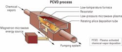
First, the high molecular velocity created by microwave-generated plasma enables very rapid direct deposition of consolidated glass. Second, the deposited glass layers in the core of the fiber are extremely well controlled, thin, and consistent from one end of the preform to the other. Third, the substrate tube is kept at a consistent and much lower temperature than MCVD. That avoids the thermal distortions caused by MCVD’s external localized flame heating. The PCVD process is illustrated in Figure 1.
As the PCVD resonator traverses the rotating silica deposition tube, the gas composition is altered with each pass and a submicron layer of glass with a precise index of refraction is created. The final RIP thus comprises thousands of precisely controlled layers.
Another feature of the PCVD process is that the microwave energy is transferred to the gas mixture without any energy loss to the silica deposition tube. Consequently, the speed of the resonator along the tube is very fast; several thousand very thin glass layers can be deposited faster than the hundred or so thick layers deposited by the slower MCVD. As a result, the PCVD process creates a nearly perfect index profile and consequently the highest-bandwidth and tightest DMD-profile MMFs.
Furthermore, by keeping the process parameters much more consistent along the length of the preform, the composition of the core glass and resulting fiber is much more consistent. That results in very high manufacturing yields, lower cost, and extremely low fiber-to-fiber variability, which is advantageous in applications like high-density ribbon interconnects and parallel data links requiring very low skew.
In addition to the hyperfine RIP control guaranteed by the PCVD process, the physical geometries of the core and cladding are also very tightly controlled. The very high molecular velocity, low-pressure microwave plasma is localized inside the tube. That allows the substrate to be maintained at a temperature much lower than its softening point, avoiding deformation, sag, and out-of-round variability. This precise and consistent fiber geometry results in lower, more consistent insertion loss and higher, more consistent concatenated bandwidth.
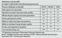
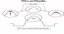
Once all the required layers of glass are deposited on the inside wall of the substrate tube, it is collapsed into a solid rod or “core perform”-a very critical step in preform fabrication. Processes that require externally applied high temperatures for tube collapse or sintering can cause dramatic degradation of the RIP. The high temperature “boils off” germanium from the inside layers, erratically reducing the index of refraction in the very center of the core. That causes high and unpredictable modal dispersion, which results in low and inconsistent bandwidth. This degradation of the index profile is commonly known as the “center dip” and is a performance limitation for some MMFs (see Figure 2).The inventors of PCVD eliminated the center dip in 1984, and practitioners continue to produce the near-perfect index profile required for ultra-high-bandwidth fiber. The Table summarizes the process attributes for the major core preform manufacturing processes: PCVD, MCVD, and OVD.
The growing market requirement for 10-Gbit/sec applications is driving all fiber manufacturers to find ways to optimize their production technology to produce high-performance 50-µm MMF at higher yields. The challenge will be to produce this fiber with a bandwidth sufficient to support transmission rates beyond 10 Gbits/sec at commercially viable yields. And with 10-Gbit/sec applications now gaining momentum in the market, it is likely that standards bodies will begin considering the next increase in transmission rates by late next year or early 2007. Line rates in premises backbones will likely increase to 40 Gbits/sec, and a key question is whether MMF will be able to transmit at this rate over 300 m.In the same work, IBM evaluated the effect of fiber-to-laser misalignment on the bandwidth of the fiber. One of the main advantages of multimode over singlemode fiber (SMF) is the ease of alignment of the optics due to the former’s larger-diameter core. Bandwidth degradation can occur due to the offset of the source relative to the fiber as well as fiber-to-fiber offsets. The PCVD fiber tested did not exhibit any bandwidth degradation when the source was offset. That further indicated a very flat DMD profile for the PCVD fiber.
The data generated by this research suggested that the 10-Gigabit Ethernet standard might be conservative and that this low-cost technology has the potential to be extended to 40 Gbits/sec. That would enable ultra-high-bandwidth 50-µm MMF to continue to serve the premises backbone market and eliminate the need for a transition to SMF and costly singlemode transmitters.
PCVD continues to provide an ideal manufacturing platform for ultra-high-bandwidth MMFs. The PCVD process has been optimized over the past 20 years. Currently, 50-µm fiber with bandwidth exceeding 11,000 MHz•km is being realized in a manufacturing environment. Bandwidth performance of 15,000 MHz•km appears to be easily achievable in the near term, with the potential for 300-m 40-Gbit/sec links possible in the longer term.Crawford Cutts and William “Bill” Beck are sales representatives for Yangtze Optical Fiber and Cable Co. (YOFC-Wuhan, China) in North America. Beck also is president-elect and program chair of the New England Fiberoptic Council. Raadjkumar Matai is technical director and Luo Jie is the R&D manager at YOFC.
PCVD for specialty optical-fiber designsThe plasma-activated chemical-vapor deposition (PVCD) process is a very powerful manufacturing platform for the fabrication of specialty optical fibers, thanks to the “hyperfine” refractive index profile (RIP). Think of the fiber RIP as a mathematical function or even an arbitrarily defined curve. PCVD can directly deposit glass compositions that fit such curves with incredible precision. For example, PCVD can dramatically increase the bandwidth of graded index multimode fibers (MMFs) for special nonstandard applications such as ultra-long-reach (ULR) high-definition video (HDV) links. Transmission rates of 2.5 Gbits/sec over 5 km of PCVD MMF have been achieved, enabling the use of low-cost transmitters and low-bending-loss cables for HDV field links.
PCVD can achieve very high refractive index differences, so-called “delta n” values. Extremely high levels of germanium can be incorporated in the core and high levels of fluorine can “down-dope” the cladding, resulting in extremely high numerical aperture fibers for sensors and illumination applications.
Hyperfine RIP control can be applied to specialty singlemode fiber designs as well. Second-generation dispersion management fibers with extremely complex and well-controlled index profiles are made with over 9,000 deposited layers, achieving very high levels of dispersion compensation and extremely low attenuation. These fibers can be used as dispersion management network elements with the twin benefits of minimized span loss and low transmission latency. They could dramatically improve the performance and cost of ULR systems.
Finally, the combination of hyperfine RIP control with similarly hyperfine rare-earth dopant control holds promise for powerful new families of hybrid fibers that perform multiple functions with high efficiency.


