Optical backplanes show dynamic growth potential
Jeff D. Montgomery, ElectroniCast Corp.
The use of optical fiber for signal interconnection began with the simplest level of point-to-point fibers in telecommunications long-haul networks. Now, as telecommunications rapidly becomes more sophisticated, the method of interconnection must adjust to keep up with complex optical-interconnect circuits and increasing numbers of optical-communication channels-whether optical fiber, planar optical waveguide, or free space. As a result of this expansion, optical backplanes are dis placing fiber cable jumpers for short-distance, high-density applications.
Connections are usually made from the optoelectronics on printed wiring boards or cards-which are, in turn, on shelves of cabinets-to those on other boards on the same or other shelves. Other types of optical interconnections are between cabinets of multicabinet equipment (such as digital crossconnect switches) or between the central processing units and remote memories of high-performance workstations and computers. The term "remote" can range in meaning from a few centi meters to tens of meters.
In the past, interconnections were made with short optical-fiber cables, called "jumpers," or patch cords. However, the increasing density of these cable connections is creating problems in cable management, resulting in incorrect or unidentified connections. Other trouble spots include reliability, cost, and space consumption. As a solution, equipment-packaging designers are turning to a technique previously developed for high-density electronic and power interconnections: backplanes and their attendant motherboards and daughterboards.
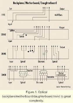
Most of the current consumption of optical backplanes consists of relatively simple optical-circuit layouts. As volume increases, consumption will tend toward increasingly complex circuits, as illustrated in Figure 1. These backplanes also will incorporate active and passive optical and electronic components, moderating the downward plunge of average prices of overall optical functional categories.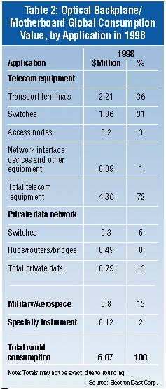
The early global demand for optical backplanes is mostly in telecommunications equipment, as shown in Table 2. The most explosive demand is in fiber-optic links for telecommunications access networks. These are for relatively short distance (hundreds of meters to a few kilometers), and mostly at moderate data rates (155 Mbits/sec to 2.5 Gbits/sec). Production quantities are anticipated to be high (millions per year) and the designs will be relatively standardized.
Private-data network (data-commmunications) applications of optical backplanes for fiber-optic links are also expected to rise rapidly over the next decade. In this market, however, the shift from fiber-cable optical inter connects to optical backplanes and motherboards will lag behind telecommunications applications. In data communications, the use of optical backplanes and motherboards in hubs, routers, bridges, and computers is the most popular application, with an 8% value share in 1998. Intracomputer optical interconnect backplanes (counted within the datacom hubs/rout ers/bridges category) is forecasted to quickly expand over the 2003-2008 period.
The factory cost of an optical backplane or motherboard consists of the cost of its various components, plus the assembly and testing labor cost, plus factory overhead. The sales price must cover the factory cost. It must also cover sales, administrative, and general costs, plus profit. So the components' cost contribution is a relatively moderate share of backplane sales/consumption value.
The market for optical backplanes and motherboards is price-elastic. Falling prices will be more than offset by growth in quantities shipped. Component producers, therefore, are focusing on ways to reduce production costs. The factory cost of optical backplanes is projected to include its cost outlay in the alignment, positioning, processing, and testing required.
Generally, the higher the performance requirements, and the more complex the circuits, the higher the fabrication/assembly costs. Much of the fabrication/ assembly cost consists of the cost of human labor. Automation can greatly reduce this labor cost. And over the next 10 years, as passive assembly automation greatly reduces the labor cost contribution, the relative value share contributed by components should expand.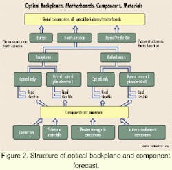
Fortunately, the assembly/fabrication processing of optical backplanes is similar to procedures used in electronic backplane and motherboard production. Electronic backplanes and boards are produced in a wide range of production lot quantities and sophistication levels. At the extreme high end are multilayer assemblies; fine-line, high-density, tight-tolerance circuit patterns; and polyamide and other high-performance materials. Single-layer, paper-laminate-based, simple-circuit boards produced for consumer electronics are at the opposite extreme. Production facilities range from high-volume, low-cost-per-unit plants to specialty shops that produce a few, very complex, expensive boards per day. The various types of optical backplanes and motherboards can be phased into appropriate existing plants. The supporting components, however, are highly specialized and will offer markets for new vendors.
Beyond cost reduction, fabrication/assembly automation provides other advantages. Quality control can become more effective with the elimination of human vagaries. Wide swings in output volume can be more easily accommodated.
Major advances have been achieved in the technology of fabricating an optical waveguide in polymeric film over the past 15 years. Several companies made major advances in this field through the 1980s, but the technology was ahead of the applications. Applications were ad vanced over the past five years by development of several short-distance, harness-style, massively parallel optical interconnects. Optical and mechanical/ environmental performance is now adequate for the dimensions of optical backplanes and motherboards. For applications involving large quantities of complex, short-distance optical interconnections (amenable to photolithographic processing), polymeric-film optical-waveguide substrates will gain strong acceptance.
Flip-chip packaging technology has been in existence for more than 30 years, and it has evolved to encompass a wide variety of materials and techniques for bumping, attaching, and underfilling die. Many options are now available for flip-chip packaging, and designers are using flip chips to solve the problems associated with higher frequencies and tighter space requirements of modern telecommunications technology.
A recent addition to flip-chip production technology is polymer packaging using conductive epoxy bumps instead of solder. Polymer bumping allows lower temperature processing than solder bumping. This, in turn, allows the use of a variety of substrate materials that could not withstand solder flow temperatures. Polymer bumps can also withstand thermal cycling.
Many different substrates have been used in flip-chip packaging. Ceramic substrates are used to handle the greater heat that high input/output flip-chip devices generate. Regular printed circuit boards and flex circuits are satisfactory substrates for low-power applications. Organic laminate substrates are also being used.
Lack of standardization and the high cost are currently the main roadblocks to widespread use of flip-chip devices. Another handicap is that the infrastructure for manufacturing, testing, and handling flip-chips from semiconductor vendors is not yet mature.
The current surge of lightwave communication into high-volume interconnection to homes, desktops, and small businesses, as well as the related expansion of feeder, interexchange, and long-haul trunk optical channels, is driving an explosive growth of transmitter-to-receiver interconnections.
The global consumption of components (parts and materials) in optical backplanes and motherboards is forecast to reach $331 million in 2008. The leading share of this amount will be accounted for by optical and hybrid connectors. Dynamic growth also will be achieved by substrate materials and embedded active optoelectronics.
This growth and future large value demand will provide the profit potential to fund the development and product marketing of optical backplanes and their supporting components and materials.
Jeff D. Montgomery is chairman of ElectroniCast Corp., a consultancy in San Mateo, CA. This article appeared in the December 1999 issue of Integrated Communications Design, Lightwave's sister publication.
ElectroniCast uses a two-level analysis and forecast of the current and future global consumption of optical backplanes as well as the components used in their fabrication. The structure of the analysis is shown in simplified form (see Figure 2). The structure includes subsets of the end-use equipment, backplanes, and components. For each major world region, the consumption of each type of backplane/motherboard in the production of each equipment subset is forecast.
Additionally, the consumption of each type of component and material in the fabrication of each optical backplane type is forecast. The quantity of consumption of each component type in each year is forecast, linked to the optical backplane/motherboard quantity forecast.
Optical backplane: A planar assembly of optical waveguide(s) that interconnect via demountable connectors from optoelectronics on a motherboard to optoelectronics on another motherboard in the same equipment shelf or to optical waveguide(s) that in turn connect to optoelectronics on another shelf in the same equipment, or that are external to the equipment. May be either rigid or flexible. Optical waveguide may be fiber, or processed in polymeric film or other material. Excludes planes which do not incorporate optical wave guides, but serve only as a mounting surface for optical feed-through connectors.
Optical motherboard: A planar assembly of optical waveguides, with edge-mounted demountable connector(s) for interfacing to an optical backplane. May incorporate optical waveguide for optical interconnect from the optoelectronics to the edge connector. May also incorporate other optical components. May be rigid or flexible.
Hybrid optical backplane (or motherboard): Same as optical, except also incorporates electrical connector channels, plus may include electronic components and optoelectronics.