Chipping away some of the cost and complexity of the optical layer
G. F. Lipscomb Lightwave Microsystems
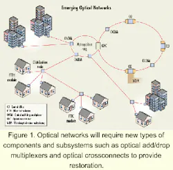
Data traffic in telephone networks worldwide is growing exponentially, while voice traffic is increasing linearly at about 7% to 10% per year. Consequently, data traffic will soon overwhelm voice transmission. By some accounts, data traffic is doubling every 12 months. In turn, the capacity of telephone networks must also grow extremely rapidly. The technology enabling carriers to accommodate this explosion of bandwidth, at least in the long-haul network backbone, is dense wavelength-division multiplexing (DWDM).After its initial success, it was not long before developers began to envision more powerful uses for DWDM beyond its role as a "dumb" fiber multiplier. In many different companies and laboratories, the concept of an "all-optical" network was born (see Figure 1). Argument still rages as to whether the all-optical network should be "transparent," "opaque," "digital," or "analog." However, the common vision is a network where high-bandwidth, optical data streams flow unobstructed-only broken down into their substituent electronic digital parts where absolutely necessary.
Emerging optical networks require many more optical components, and different types of components, than point-to-point systems. Today's 80-channel systems with dual-band amplifiers are very complex. For example, an 80-channel point-to-point system with three amplifier stages can require 281 passive components, compared to only 13 for a 4-channel system. Similarly, active-component counts could reach 240, up from eight for a 4-channel system. To manage and protect such complex systems requires new types of components and subsystems. For example, optical add/drop multiplexers (OADMs) make provisioning of such massive bandwidth efficient; optical crossconnects provide restoration and protection as well as provisioning.
Optical networks are extremely expensive and much of the cost is in the optical components used in the system. For the "all-optical" network to become a reality, optical-component costs must drop dramatically. One approach to reducing this cost is through integration of multiple functions in a single package. Planar lightwave circuits (PLCs), broadly defined, are the platform on which these integrated components can be built.
PLCs are optical circuits constructed of waveguides laid out on a silicon wafer, made using advanced tools and techniques developed by the semiconductor industry. With this process, developers can fabricate and interconnect multiple components at once, significantly reducing both the manufacturing and packaging/assembly costs.
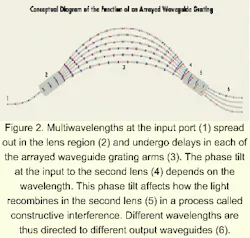
Waveguides and devices can be fabricated using either glass or polymer materials. Using different geometries, waveguides can also be made from semiconductors such as indium phosphide (InP) and silicon or from inorganic crystals such as lithium niobate (LiNbO3). Each material has advantages and disadvantages for a given function. Based on the material and design, waveguide devices can be fabricated to perform many different optical functions. Table 1 provides a summary of the types of materials used for making optical waveguides.Fairly complex optical PLC components are already in widespread commercial use. Since arrayed waveguide gratings (AWGs) were first proposed by Smit1 in 1988, extensive work has gone into applying this technology to DWDM applications.2, 3 A conceptual diagram of the function of the AWG is shown in Figure 2.
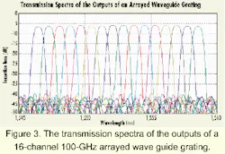
AWGs are commonly used for multiplexing or demultiplexing 16 channels with a separation of 100 GHz between channels, thus representing in and of itself a fairly high degree of integration. The same function performed with thin-film filters would require 15 different filters, each with their associated beam expansion and refocusing optics (more than 45-piece parts). AWGs with 40 channels spaced at 50 GHz are commercially available. An AWG with 128 channels spaced at 25 GHz has been demonstrated in the laboratory.4When viewed from the perspective of what is placed on the chip, the level of integration is also impressive. For the AWG to perform properly, each of the more than 100 optical elements on the chip must perform precisely. Such is the power of photolithography and semiconductor manufacturing techniques that once the design is correct and the manufacturing process stable, these optical circuits can be manufactured in high volume. The transmission spectrum of each of the output waveguides of a 16-channel 100-GHz AWG is shown in Figure 3.
Active functions such as optical path switching are also critical for emerging optical networks. When a single optical fiber can carry 100s of Gbits/sec to 1 Tbit/sec, instead of a mere 2.5 Gbits/sec, it is desirable to perform network-management functions such as protection, restoration, and grooming on the entire optical stream, without transforming the data back into the electrical domain and without detecting individual packets. This approach is possible using an optical path switch that redirects all of the light in an input fiber to an output fiber.
The simplest example of optical switching is 1:1 protection. In this case, a "working" fiber and a "protect" fiber, which follow different routes to the same destination, are connected to the network with two 1x2 switches. If the "working" fiber is cut or damaged, the 1x2 switches automatically reroute the optical data stream to the "protect" fiber. Of course, in actual practice, even this "simple" example presents many system challenges such as how to detect a system fault, but that is the subject of a different article. Many complicated architectures have been proposed, which place even greater demands on the optical switches. In an effort to meet these challenges, the following technologies have been used to make optical switches:
- Optomechanical
- Beam steering
- Liquid crystal
- Polymer thermo-optic
- Silica thermo-optic
- Micro-electromechanical (MEM)
- Frustrated total internal reflection (FTIR)
- LiNbO3
- Semiconductor (InP)
- Semiconductor optical amplifiers (SOA)
Thermo-optic switches based on silica or polymer waveguides are made using PLC fabrication techniques and are commercially available in integrated arrays from several vendors. Because standard wave guides are used, these thermo-optic switches can be monolithically integrated with other passive and active waveguide structures on a single substrate. Integration with other switch technologies is also possible but usually requires some form of hybrid assembly. The ability to integrate different functions on a single substrate opens up the possibility of performing higher-level network operations within a single package.
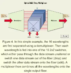
Many different optical functions are required to make an optical-network module or subsystem. One example is a reconfigurable OADM, which is considered a critical element for emerging metro systems, where flexibility of deployment is one of the drivers for using DWDM technology. A simplified, 16-channel, reconfigurable OADM is shown in Figure 4. (An actual system would require additional parts for monitoring and power leveling.) In this simple example, the 16 wavelengths are first separated using a demultiplexer. Then each wavelength is fed into one of 16 2x2 switches, which either pass the data stream through unaltered-the bar state-or switch one data stream out of the fiber (drop) and switch another data stream onto the fiber (add)-the cross state. A multiplexer then combines all of the wavelengths onto the single output fiber.
If this module were constructed using discrete parts-counting the multiplexer and demultiplexer as one part each-it would require 18 components with a total of 98 fiber input/outputs (I/Os) in the packages. Moreover, 32 fiber splices would be necessary to connect the parts together. If variable optical attenuators (VOAs) are added to each output channel, as is required in some applications, the number of components increases to 34, the fiber I/Os needed is 130, and the number of splices jumps to 64. Based on the number of components and the complexity, the manufacture and assembly of this module is quite expensive. It is critical to reduce this cost for wide deployment of reconfigurable OADMs in metro systems.Indeed, optical integration in PLCs has the potential to dramatically cut the cost of optical modules such as OADMs. All of the OADM functionality has been demonstrated and deployed in a single PLC. If the entire structure is on one chip, the manufacturing, packaging, and assembly costs are reduced. For example, the OADM shown in Figure 4, even with VOAs, would become a single integrated component that requires only 34 fiber I/Os in the package and no fiber splices for assembly. Of course, the OADM would still have to be connected to the network and the drop/add ports. Such integrated OADMs have been demonstrated in silica wave guides5 and in polymer waveguides.6
The OADM is just one example of an optical module that can benefit from integration of multiple elements on a single substrate. Groups around the world are working to utilize the many possible PLC functions to make integrated modules. Recent demonstrations include an integrated dynamic-gain equalization chip,7 an integrated multichannel waveguide laser,8 and a frequency-spectrum synthesizer.9 Several vendors will release second-generation products later this year that will replace rack-mounted boxes of traditional optical components. Future products will integrate multiple optical functions, including lasers, receivers, and electronics, inside the package.
It is possible to reliably manufacture these complex PLC devices in high volumes by capitalizing on the extensive infrastructure created by the silicon integrated-circuits industry. This infrastructure consists of the equipment, processes, and methodologies that have been built up over 40 years with the investment of billions of dollars.
It is also important to recognize the limitations of optical integration in PLCs. The wave lengths of in terest to tele communications companies are 10,000 times the size of an electron. Different levels of optical integration will be limited to hundreds of elements, a small number compared to the millions encountered in electronic integrated circuits. Nonetheless, there is much to be gained over current discrete optics, and PLCs represent the next level of efficiency and performance in fiber-optic components.
For fiber-optic technology and DWDM to continue to migrate from the backbone out to the metro networks and beyond, the performance and cost efficiency must increase dramatically. By integrating many functions in a single package, PLC technology can achieve this performance enhancement.
G. F. Lipscomb is vice president of marketing at Lightwave Microsystems Corp. (San Jose, CA). The company's Website is www.lightwavemicro.com.
- M.K. Smit, "New focusing and dispersive planar component based on an optical phased array," Electronics Letters, 24, 385 (1988).
- H. Takahashi, "Arrayed Waveguide Grating for Wavelength Division Multi/Demultiplexer with Nanometer Resolution," Electronics Letters, 26, 87 (1990).
- C. Dragonne, "Integrated optics NxN multiplexer on silicon," IEEE Photonics Letters, 3, 896 (1991).
- K. Okamoto, K. Suto, H. Takahashi and Y. Ohmori, "Fabrication of 128-channel arrayed waveguide grating multiplexer with 25 GHz channel spacing," Electronics Letters, 32 1474 (1996).
- K. Okamoto, M. Okuno, A. Himeno and Y. Ohmori, "16 channel optical add/drop multiplexer consisting of arrayed waveguide gratings and double gate switches," IEEE Photonics Letters, 32 1471 (1996).
- G. Beelen, P. Linders, C.G.H. Roeloffzen, A. Driessen, M.B.J. Diemeer, X.J.M. Leijtens, A.F. Bakker and A.G.T. de Krijger, "First polymer based reconfigurable add-drop multiplexer," ECOC'00 Post Deadline Papers, p. 58.
- B.J. Pffrein, G.L. Bona, R. Germann, F. Horst and H.W.M. Salamink, "Dynamic Gain Equalization in High Index Contrast SiON Technology," ECOC'99 Post Deadline Papers, p. 6.
- M.W. Sckerl, S. Guldberg-Kjaer and Chr. Laurent-Lund, "Monolithic DWDM Multi-Channel Planar Waveguide Laser," ECOC'99 Post Deadline Papers, p. 16.
- K. Okamoto, T. Kominato, H. Yamada and T. Goh, "Fabrication of a frequency spectrum synthesiser consisting of arrayed waveguide grating pair and thermo-optic amplitude and phase controllers," Electronics Letters 35 (April 1999).


