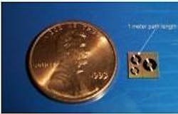
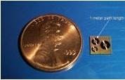
Optical time delay circuits feature ultra long path length
5 September 2003, Annapolis Junction, MD Lightwave --Little Optics, Inc., a developer of high-index optical waveguide materials for planar lightwave circuits (PLCs), is taking orders for compact, ultra long path length time delay circuits based on its patented Hydex material system. Long path length time delay circuits are of increasing interest for phased array antennae, optical switching, optical clock distribution, optical time domain multiplexing, polarization mode dispersion compensation, differential phase shift key, optical pulse replication, and sensor applications.
The company claims that its ability to miniaturize complex PLC circuits to <1 cm2 leads to dramatic improvements in cost, performance, functionality, and size. This combination of features makes the use of PLC circuits economically viable to a broader range of applications than previously possible with conventional low-index PLC processes.Little Optics offers two architectures for time delay circuits: a multi-stage programmable delay line up to 64 bits and an unbalanced Mach-Zehnder interferometer with differential path lengths up to 2 m. These devices are fabricated on the company's patented high-index glass platform (i.e., core/clad index contrast ratio up to 25%), resulting in hundreds of die per 6-inch wafer, the company claims.
Compared with conventional low-index processes, Little Optics lists the following benefits of the Hydex material system:
1. Increase of optical path length up to 1,000x.
2. Decrease in chip size by 10-50x.
3. Flexible "pick and place" stepper lithography techniques that allow stitching of long-path-length spirals to common device architecture.
4. Increased number of optical circuit elements per die.

