Memory chip puts lasers in a spin
Scientists in the Netherlands have developed a fast optical memory element based on coupled micro-ring lasers.
By JAMES TYRRELL
Optics.org
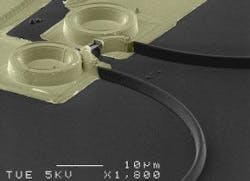
Researchers in the Netherlands have developed a fast low-power optical memory element that exploits the clockwise and anti-clockwise lasing properties of ring cavities. The bistable device, which switches between the two modes within 20 psec and occupies an area of 18 x 40 μ m2, could form the building block for future high-speed optical processors.
Micro-ring lasers typically have two inherent lasing modes--laser light traveling in the clockwise (CW) direction and laser light traveling in the anti-clockwise (ACW) direction. By connecting two ring lasers together via an optical waveguide, the team exploits these CW and ACW properties to create a system with two stable states.
"We can switch between states by injecting a laser pulse," explains researcher Martin Hill from COBRA research institute, Technische Universiteit Eindhoven. "Because it is small and low power, you can have lots on a chip working together at high speed."
To demonstrate the concept, the team fabricated two micro-ring lasers (A and B) measuring 16 μ m in diameter on a wafer containing active InGaAsP material emitting at 1.55 μ m. The width of the ring and inter-laser ridge waveguide was 2 μ m.
The system works by using 13-psec duration pulses of light, sent along the interconnecting waveguide, to force the system to lase in one of two states. In the first state, light from laser A injection-locks laser B, forcing it to lase only in the CW direction. Conversely, in the second state (activated by sending a pulse in the opposite direction), light from laser B injection-locks laser A, forcing it to lase only in the ACW direction. The different states are detected by a change in power level at the two inputs/outputs.
"In itself it is a simple function that you could use for memory or threshold functions such as a gate," notes Hill. "However, the idea is to use it as a building block to construct more advanced non-linear functions in optical-digital systems."
By densely integrating and interconnecting large numbers of these devices, the group hopes to develop high-speed optical processors, which could be used in areas such as the telecommunications sector, replacing electronic based logic operations within fiber networks to boost data rates.
The team is conducting its research with support from the Netherlands Organization for Scientific research (NWO). JDS Uniphase supplied wafer materials for the project. Currently, the researchers are working with Korean colleagues to develop photonic crystal technology, which they hope can be used to shrink the size of the laser down to 1 μ m and below.
• This article originally appeared on Optics.org.
James Tyrrell is a reporter on Optics.org and Opto & Laser Europe Magazine.

