Material world: Integration advances drive metro and access DWDM
New integrated-device technologies will create the migration path, enabling smaller, cost-effective components.
Dr. Gary C. Bjorklund and Dr. Wei-Ping Huang
Nanovation Technologies
As optical networking moves into the metro and access arenas, manufacturers will utilize advances in integration to design components and build DWDM systems that fit these networks' requirements. The properties of materials will play an important role in this migration.
As long as fiber-optic communication systems are made of silica, there will be a need for pure silica planar-waveguide devices for passive functions. However, as material and design technologies evolve, silica will be combined in a hybrid manner with other materials such as indium phosphide (InP) for more functionality. Creating hybrids means that passive and active devices as well as purely electronic devices will be come smaller, more efficient, and more cost-effective-all critical features to the success of DWDM in metro and ac cess environments. Materials such as silica-on-silicon and hybrids such as silica/micro- electromechanical systems (MEMS) will play an important role in applying DWDM to metro and access networks.
Despite the promise of new, innovative materials for metro and access DWDM devices, silica will be a mainstay in device design for passive planar-waveguide devices. Silica is particularly attractive as the base material for optical communication components because of its inherent compatibility with standard optical fibers, resulting in low insertion loss and polarization insensitivity.
Furthermore, the manufacture of planar, silica-based waveguides offers the potential for mass production and capitalizes on the same processing techniques developed for semiconductor circuits, making it possible to integrate much functionality in a single component. The result is economical devices produced en masse, a critical market factor that will not only drive the metro and access DWDM loop, but also propel the technology straight to the desktop.
Silica itself has a bright future for metro and access DWDM applications. However, by integrating it with new, more advanced technologies, device designers will have more freedom in meeting market demands for advanced devices.
Hybrid silica/ MEMS will play an im portant role in making metro and access DWDM networks a reality sooner rat her than later. Silica/ MEMS technology offers a sensible way to create network equipment that is capable of reconfiguration and protection in metro and access DWDM networks.Most recently, optical MEMS technology development has been primarily focused on either free-space or large-array switching, because all-optical-crossconnect switching is in demand and absolutely necessary to break the network bottleneck of optical-to-electrical-to-optical conversion that is required to route the communications traffic. Hybrid/silica MEMS technology extends that solution to the edge of the network. By combining materials best suited to perform the specific optical functions needed for DWDM systems and fabricating them with standard chip-manufacturing techniques used for ordinary integrated silicon circuits, custom-designed, integrated planar metro and access DWDM systems can be created quickly and cost-effectively. Examples of metro and access DWDM components based on hybrid/silica MEMS technology include new protection-switching circuits, optical-wavelength add/drop multiplexers, and network-performance monitoring systems with densities improved 20 times over existing chipsets. As a result, a full rack of equipment can be reduced to a single rack-mount shelf. This space-saving feature is important, because space allotted for metro and access switching equipment is limited and expensive.
This flexible design architecture enables device manufacturers to easily create custom devices. This technology can be produced with the same manufacturing processes used for semiconductors. The result is a reliable mass-production chain that will increase the supply and drive down costs to ensure widespread implementation of metro and access DWDM networks.
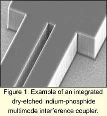
In the long run, integrated semiconductor laser diodes and optical lightwave circuit devices are key to the development of compact and low-cost DWDM systems. Therefore, the integration of III-V materials, specifically InP with different materials such as silica, is escalating in importance (see Figure 1).
InP is already the material of choice for active devices in DWDM systems. As a semiconductor material combined with silica, InP can deliver a new level of device integration that includes light generation, detection, amplification, high-speed modulation and switching, as well as passive splitting, combining, and routing.
A hybrid combination allows device designers to capitalize on the benefits of each material, while reducing the effects of the least desirable characteristics of each material's system. For example, InP shortens interconnections, because the waveguides can be routed with very small bending radii. But with InP integration, the insertion loss tends to be high, and because waveguides are much smaller compared to singlemode fibers, the coupling efficiency between the fiber and the waveguide is low. Silica doesn't have this power, so the drawbacks of InP are greatly reduced.
These integrated, highly flexible devices will result in very small, futureproof, high-speed switching systems suitable to intricate customization. By employing the same fabrication processes and mass-production techniques used for silicon microelectronics, InP/silica integrated circuits will offer more diversity in creating smaller, faster, cheaper, and more functional devices for the metro and access DWDM marketplace.
With all the advantages made possible by silica/MEMS and InP, designers will have a hard time getting their arms around the new advances fast enough to meet market demand. Therefore, they must rely on advanced computer-aided design (CAD) tools to bring it all together.
CAD is not a new concept in device design. What is new, however, is the urgency with which photonic devices must be created and the rapid introduction of new material integration techniques like silica/MEMS, for example. This urgency, coupled with a fragmentation within the capabilities of CAD tools, leads to a frustration that begins in the design lab and rumbles through the entire industry.
To create next-generation photonic devices based on new material combinations with the tempo, precision, and cost-effectiveness necessary to keep pace with market demand, designers need an end-to-end CAD system with on-board knowledge of the basic photonic foundations of these new materials.
By using a CAD system that combines device and circuit modeling within a hierarchical framework and a common database that shares information within individual design steps, designers achieve a more direct and efficient approach in creating a complete component. A vertical, clearly segmented approach is the most efficient way to design new photonic devices.
The core steps in any design are material design, device design, waveguide design, and circuit design. By developing the project within this logical order beginning with material design, information can be exported between levels for improved speed, flexibility, and accuracy.
With the innovations in photonic materials, the first step in photonic design is perhaps the most critical. In this initial phase, the designer determines the performance and functionality of the finished device. For example, if the finished product is merely a passive device, the designer might select silica. If the device is a more complicated passive device, silica/ MEMS would be a better choice, and InP would be selected for active devices.
Suppose the device is more complicated: an integrated active device for metro and access DWDM applications that is powerful enough to bring information from the long-haul network to the building. Would this be InP or gallium arsenide, lithium niobate or another advanced III-V material? Which is the better choice to meet the design goals? The quickest way to solve the problem would be through an on-board knowledge base, available through the CAD software itself.
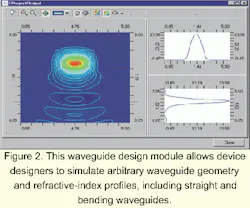
Once the material design is completed, the waveguide design must be developed. Like the material module, the CAD should provide a predefined library of waveguide structures. By vertically importing the foundation formed in the first step, designers should be able to swiftly process waveguide geometry and random refractive-index profiles for both straight and bending waveguides (see Figure 2).The waveguide design tool must also accurately compute basic and higher modes, guided and leaky modes, and semivector and full-vector modes. Other features to consider include confinement factor, far-field pattern, overlap fields, alignment, facet calculation, and equivalent index.
From there, the designer should be able to progress to the design of the device itself, building directly on previously created designs. Many disparate device design tools are available, but the most advanced software packages include templates and knowledge-based libraries, offering a logical starting point. With a template, the designer can build the device around a predefined structure to meet specific goals in terms of functionality and performance.
Other design performance features to consider include advanced wave-propagation solvers for device simulation, reflection, transmission, radiation loss, polarization-dependency loss, group delay, dispersion loss, power-splitter ratio, and phase difference between ports.
The photonic integrated circuit is the last stage in the design of a photonic device. Few CAD packages accommodate photonic integrated-circuit design, which should be taken into consideration when evaluating CAD suites.
As the final step in device design, circuit packaging is critical because it reduces the hefty resource costs associated with prototype development.
Neural-network technology is critical, particularly when dealing with new material integrations. Neural networks generate meaningful connections between processing elements, instead of merely processing information, essentially learning from previous simulations and examples. The result is faster, more accurate response to simulation tasks.
From the integration of materials to the integration of circuits, the light spectrum is being pushed farther and faster than ever predicted. First across the country, now across town, there are a multitude of issues to consider when creating the foundation of metro and access DWDM systems. Because of size and functionality limitations, few of today's material solutions will do. Therefore, researchers are leveraging new integration techniques as well as reliable standbys such as silica to create material systems specifically focused on the needs of metro and access DWDM applications.
Once these materials are in place, designers need an advanced suite of tools with an inherent knowledge of how these materials will function within the devices created specifically for metro and access DWDM. By considering the entire process from material development through circuit modeling, equipment manufacturers will be able to develop effective product strategies to meet escalating market demands for bandwidth.
Dr. Gary C. Bjorklund is chief technology officer and senior vice president of Nanovation Technologies, and Dr. Wei-Ping Huang serves as senior vice president for the indium-phosphide business unit at Nanovation Technologies (Miami).
Get Answers-Fast!
To get the quickest response to your question, contact the appropriate person listed below.
Reprints, Bulletin Board
Kathleen McIntosh
Tel: (603) 891-9203
E-mail: [email protected]
Subscriptions, back issues
Michelle Blake
Tel: (603) 891-9360
E-mail: [email protected]
New Products, Calendar
Leah Gladu
Tel: (603) 891-9219
E-mail: [email protected]
News and features
Stephen M. Hardy
Tel: (603) 891-9454
E-mail: [email protected]
Media kit, editorial calendar
Hilary Lloyd
Tel: (603) 891-9218
E-mail: [email protected]
Paid subscriptions
Omeda Customer Service
Tel: (847) 559-7520
E-mail: [email protected]


