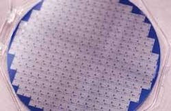
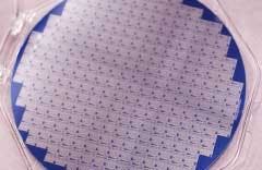
Bandgap structures move to wafers
According to Giorgio Grosso, chief executive of Pirelli Labs, the combination of nanotechnology and bandgap structures promises to deliver integrated devices in much smaller packages than conventional technologies can provide. Companies such as NanoOpto (Somerset, NJ) already have introduced the concept of nanotechnology—the creation and application of structures in sizes of less than a micron—to optical communications (see "Manufacturing optical components on a nanoscale," Lightwave, October 2002, page 52). However, Pirelli is among the first to pair this technology with bandgap structures at the wafer level. The thrust holds a fair degree of risk since both technology areas have just begun to see commercialization.
Bandgap technology—also referred to as "photonic crystals"—offers an alternative way of guiding light down a waveguide. Most waveguides in today's commercial products, including fiber, rely on differences in refractive index between two solid materials (such as the core and cladding of a fiber) to keep light moving in the intended direction and with the desired properties. Photonic bandgaps operate much in the same way as the electronic bandgaps in semiconductor materials. In electronic bandgaps, electrons that lack a certain level of energy are blocked; similarly, photonic bandgaps block photons of target frequencies.
Most of the work in photonic-bandgap technology has centered on using the concept to control the transmission of light through fiber. Researchers introduce microstructures into the fiber to create such bandgaps. The most commonly discussed of these structures is an air gap, or a series of gaps, which creates the fairly well known result called "holey fiber."
Pirelli, working in conjunction with the Microphotonics Center of the Massachusetts Institute of Technology, has moved the research focus from fiber to wafer-level waveguides. According to information posted on the center's Website (www.mit.edu/mphotonics/www/jjean.shtml), researchers at MIT have found that photonic-crystal materials—periodic composites of macroscopic dielectric and/or metallic media designed to possess an omnidirectional photonic bandgap—can be used to create microcavities, waveguides, or mirrors. Grasso says bandgap technology provides greater control of the light than convention light-guiding techniques; thus, Pirelli can create waveguides with tighter bend radii, which leads to smaller component sizes.
The use of silicon wafers also means the company can create such devices by modifying standard microelectronic manufacturing equipment, Grasso adds. In fact, it's easier to apply bandgap structures to wafers than to fiber, he claims. As with any silicon device, coupling to standard fiber is a challenge—one exacerbated by the use of the bandgap waveguides. Grasso says Pirelli Labs has overcome this potential obstacle by using tapers. While the company can create such tapers efficiently, they tend to be somewhat long, Grasso admits. The bandgap waveguides themselves are approximately 1 µm wide.
Grasso says that Pirelli will begin sampling a triplexer based on this technology early next year, with general availability in 2005. While he expects this will be his group's first high-volume product based on "nanophotonics," which the company calls the new approach, he envisions tunable and wavelength-processing filters, switches, and modulators appearing as well. So far, the lab cannot construct lasers or detectors using nanophotonics, he admits.
Which means that the product introduction that formed the focus of Pirelli Labs' exhibit at ECOC, a tunable laser, was developed by more conventional means. The continuous wave external-cavity laser does not require a wavelength locker and can support channel spacings of 25 GHz. Pirelli currently claims a switching speed of around 1 msec, although Grasso says the technology could support speeds measured in microseconds.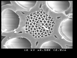
The laser will eventually be paired with a nanophotonic switching mechanism to create a module for reconfigurable add/drop multiplexing. The first version of such a device will support the adding or dropping of four wavelengths. The module will offer low pass-through loss and hitless operation, Grasso predicts. It is slated to debut next year, with general availability in the middle of next year.
Meanwhile, Pirelli has developed subsystems in conjunction with Telecom Italia that will eventually become generally available products. One of these subsystems is a "radio over fiber" unit that will allow Telecom Italia Mobile to remote microcell antennas in the field from a base station located in the central office. The subsystem will enable optical connectivity from the field antennas to the base station. The other subsystem is a CWDM device named P-MAS. Grasso says Telecom Italia will deploy the units in metro applications next year.