Photonic integration challenges in semiconductor technology
System-on-a-chip is the holy grail of integration, but several hurdles remain.
M.K. CHIN, Anadigics Inc.
Component technology development is driven by network demands. As such, work in optoelectronics began in earnest in the 1980s and '90s to create the light sources and detectors required for optical communication after low loss propagation of optical pulses in optical fibers was demonstrated. Optoelectronic devices provided the photon-electron interfaces. As networks have evolved, optical-electrical-optical (OEO) conversion speeds have increased in step with network demand for bandwidth from OC-48 (2.5 Gbits/sec) to OC-192 (10 Gbits/sec).
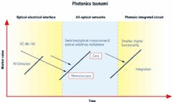
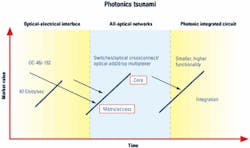
Product cycles have reflected the market push for higher bit rates in the core and cheaper components in the edge of the network. Thus, as volume for OC-48 and OC-192 parts escalates and their costs decrease, these devices are increasingly deployed in access networks, while OC-768 (40-Gbit/sec) parts are developed primarily for the network core. Figure 1 illustrates the wave-like behavior of the product development cycle.1It is possible to project some of the next technology requirements based on the direction in which networks will evolve. As networks migrate toward all-optical to eliminate the OEO bottleneck, optical switching and routing are expected to become the dominant technologies, with subsystems such as optical crossconnects and optical add/drop multiplexers (OADMs) the linchpins or "hot" products. Many competing switching technologies are being developed, such as micro-electromechanical systems, arrayed-waveguide grating, liquid crystals, fiber-based Mach-Zehnder, and fiber Bragg gratings.
However, all of these switches tend to be bulky and space-hungry and require complicated assembly and fiber management. As a result, the products demonstrated so far are not only expensive, but also are space- and power-consuming. Next-generation product development will need to drive down both cost and space. These requirements provide the motif for integration and favor technologies that are amenable to high-density integration of the subcomponents. As photonic integration becomes increasingly important in years to come, its development will focus primarily on planar lightwave integrated circuits (ICs) based on two primary materials, silica on silicon and semiconductors, especially indium phosphide (InP).
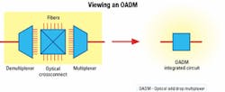
Photonic ICs (PICs), like their electronic brethren, provide many benefits such as reduced part counts, simplified packaging, lower assembly cost as well as increased functionality and reliability, especially in all solid-state technologies. The overall cost is lower, which will drive additional applications and more integration.A prime example of very-small-scale integration is between an electroabsorption modulator and a distributed-feedback laser. However, the greatest power of integration may be realized only with large-scale integrated (LSI) circuits, an example of which is a high-port-count OADM. As shown in Figure 2, today's OADM is a complex system consisting of many components residing in different boxes or shelves grouped together by numerous fibers. In principle, these components can be integrated together on a single LSI chip, which can lead to smaller fiber counts and footprints-a huge cost advantage. This system-on-a-chip solution embodies the advantages of integration. Nevertheless, integration presents many challenges, among them:
- Finding a viable scheme for integrating active and passive components.
- Reducing insertion loss and polarization effects in fiber networks.
- Increasing the level of integration by shrinking device size, and process and design complexity.
The elementary passive device in integrated optics is the interconnecting waveguide, which inevitably has loss. All passive ICs will eventually be limited in size by the loss budget. To go beyond this limit would require on-chip optical amplifiers to overcome the loss, hence the need for active devices even in otherwise passive circuits.
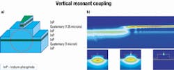
There probably is no easy way to integrate all types of active and passive photonic devices on a single substrate. Several limited approaches have been used, such as hybrid integration in the silicon-bench technology; selective-area growth, etch, and regrowth; and quantum-well intermixing in the case of InP technology. These are planar approaches in which all devices and optical beams are aligned in the same physical level. They require either complicated assembly or processes that generally degrade the product yields.In the case of InP, a mode expander region using vertically tapered waveguide structure is used to reduce the coupling loss between the InP waveguide and the fiber due to the mode mismatch. In the mode expander, light is forced to transfer from the device layer into an enlarged lower waveguide. That same function can be achieved with a relatively simple, vertical, resonant-coupling structure consisting of an upper-ridge waveguide that is laterally tapered and optically coupled to a lower and larger uniform waveguide. Since the different materials are in different layers, they can be grown in a single-step epitaxial growth, and no regrowth is needed. This structure is illustrated in Figure 3, with a simulation showing the vertical transition of light at a critical point in the tapered waveguide.
This approach can be extended to form the basis for vertical integration of active and passive devices. The design has been adopted in an asymmetric twin waveguide distributed Bragg reflector laser2 and in crosspoint switches.3 In these optical circuits, the active waveguide material lies above the passive waveguide material, and light propagates between the active and passive devices via the tapered ridge structure formed lithographically in the upper waveguide.
As the modes in the active and passive waveguides are similar in size, these tapers can be very compact, on the order of 100 microns, and thus they do not add significantly to the total length of the circuit. In addition, the two-layer design can be extended to three layers, adding a large passive waveguide at the bottom to serve as a mode expander to improve coupling of light into fiber. This method, in principle, could provide a solution to the insertion loss problem, traditionally a bottleneck for integrated optics.
The resonant tapered coupler is a versatile structure with many important advantages: It requires only one-step growth, enables vertical integration of active and passive devices, and can be used with small insertion loss.
The level of photonic integration lags far behind that of electronic integration for several reasons. First, today's photonic devices tend to be far larger than a typical transistor. Second, there is no photonic equivalent of a transistor; there are as many photonic devices as there are required functions on the chip. The different requirements on many of these devices make it difficult to achieve fully functional integration. Finally, for InP, which is the only wafer material that can be used to fabricate both active and passive devices for optical communication applications at 1.3- and 1.55-micron wavelengths, the available wafer size is still relatively small (2 or 3 inches in diameter), so relatively few devices can be fabricated on a single wafer.
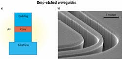
Perhaps the single largest element in an optical IC is an S-bend optical waveguide used for interconnecting devices. To minimize bending loss, an S-bend would require a radius on the order of a centimeter in the case of lithium niobate waveguide, millimeters in the case of silica, and hundreds of microns in the case of semiconductors, because all these waveguides are traditionally designed to be weakly guided (rib or buried waveguides).The conventional wisdom is that exposed sidewalls will introduce unacceptable scattering loss. However, it is precisely these deep-etched waveguides that will provide the required strong confinement of photons to enable miniaturization of interconnections. As devices and interconnections shrink, the total loss may be reduced, even though the loss per unit length may have increased. Figure 4 shows a cross section of such waveguides and the extremely small bend radius that can be achieved without significant radiation loss.
With improved fabrication technology, even the scattering-dominated propagation loss in strongly guiding InP waveguides can be kept well below 1 dB/cm provided the guide width is greater than 2 microns. Below 2 microns, the loss increases rapidly. While a 2-micron-wide ridge waveguide may be multimode, it can be used to form interferometric devices such as Mach-Zehnder, provided only the fundamental mode is excited at the input and all waveguide bends are designed appropriately to avoid mode conversion. It has been shown that certain bend shapes preserve the mode profile and hence introduce no mode conversion.
Another issue of concern for these waveguides is their polarization-dependence. Extremely narrow waveguides are strongly polarization-sensitive with the effective index higher for TM than for TE. However, the order of these effective indexes reverses as the width increases. Thus, in principle, the waveguide can be designed to be polarization-independent at a desired width, and the polarization-dependent loss will also be small as the corresponding waveguide mode is nearly circular at that point.
Another approach for shrinking the size of an optical IC is to design more compact devices through the use of novel building blocks. Some examples are the use of right-angled etched facet mirrors instead of curves to make a 90-degree bend and the use of multimode interferometers (MMIs) instead of directional couplers or Y branches to form the splitters and combiners required for optical switches. An MMI is a compact and versatile structure that can be used as a 1:N splitter, N:1 combiner, or MxN coupler.For example, a 1x4 switch can be realized as a single-stage generalized Mach-Zehnder interferometer (MZI) consisting of a 1x4 MMI splitter, a 4x4 MMI coupler, and four control phase-shifters,4 rather than a cascade of two conventional MZIs, which would have almost double the length.
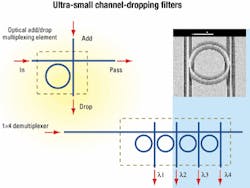
Another novel building block is a ring waveguide resonator, which can be used as a channel-dropping filter,5 an essential element for an OADM. As shown in Figure 5, a WDM signal with a band of wavelengths is passed through such a filter, and a wavelength that coincides with a resonant frequency of the resonator is switched to the drop port. To drop a unique wavelength within the signal band, the resonant filter needs to have a free spectral range (FSR) wider than the bandwidth of the WDM signal, and the ring must be very small. For InP resonators, an FSR of 20 nm requires the ring radius to be less than 5 microns. Such a small resonator can only be realized using strongly confined micro-ring waveguides or micro-disks. A series of N different resonators can be cascaded in a linear chain to form a 1:N wavelength demultiplexer.
Developers must overcome many challenges before true integration can be come viable. The commercial success of PICs requires reduction of packaging costs, improvement in process yield, and improvement in design and simulation technology. In the final analysis, a major breakthrough for PICs will occur only when both technology and the market are ready for it.
M.K. Chin is a chief scientist at Anadigics Inc. (Warren, NJ).
- M.K. Chin, paper presented in the 10th Wireless and Optical Communication Conference, Newark, NJ, April 20-21, 2001.
- P.V. Studenkov, et al., IEEE Photonic Technology Letters 12(5), 468 (2000).
- S.S. Saini, et al., IEEE Photonic Technology Letters 13, 203 (2001).
- R.M. Jenkins, et al. Applied Physics Letters 64, 684 (1994).
- M.K. Chin, et al., IEEE Photonic Technology Letters 11 (12), 1620 (1999).
