Controlled-mode interaction boosts PLC device designs
Component developers have worked on directional-coupler (DC) and Mach-Zehnder interferometer (MZI)-based structures in planar lightwave circuits (PLCs) for several years. Using these basic designs with a myriad of waveguide shaping methods, it's possible to make 1×2 and 2×2 switches, variable optical attenuators (VOAs), and optical taps. Although commercial devices have been made using DC and MZI designs, there are still multiple challenges to overcome with these designs before PLC technology becomes a market success.
Controlled-mode interaction (CMI) switching technology surpasses DC and MZI designs in many important optical performance characteristics. In addition, for any given manufacturing environment, robust CMI devices will perform better, are inherently less sensitive to manufacturing tolerances, and have higher yield. The CMI platform is well positioned to deliver on the promise of PLC technology, delivering high-performance parts at cost-effective prices.
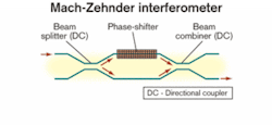
The MZI switch is based on splitting the optical beam between two waveguides, applying a phase shift on one of the beams, and finally recombining the two beams (see Figure 1). By changing the phase shift between the two arms, the interference between the beams is controlled at the output of the MZI, and that determines the switching efficiency. As any device based on optical interference, MZI is inherently sensitive to wavelength variations and any other factor affecting the optical path.
In silica-on-silicon PLC switches, the most common element that realizes the splitting and recombining of the beams is the DC. The phase-shifter is always a heater placed above one of the waveguide arms of the MZI to change the optical-beam phase via a thermo-optic effect. Depending on the phase difference between the two arms, the input light is directed to one of the output ports of the switch.
As an optical signal-switching device and a VOA, the MZI suffers from several problems that limit its manufacturability and performance in telecommunications applications. High accuracy of the phase shift and splitting ratio is very difficult to achieve for both polarizations and over the needed wavelength range. The strong polarization dependence of the phase shift is due to optical birefringence (different phase velocities for different polarizations). In addition, the splitting ratio of the DC depends strongly (exponentially) on the waveguide geometry, refractive index, and wavelength, all of which vary in accordance with manufacturing tolerances.
This sensitivity of the phase difference and splitting ratio to process variations makes the MZI-based switch difficult to manufacture. The former requires very low variation of parameters between the two MZI arms, while the latter puts stringent requirements of accuracy and repeatability on the DC section.
The crosstalk of an MZI switch depends strongly on the phase difference between the arms and on the splitting ratio. Consequently, the crosstalk of an MZI switch is typically not better than –20 dB in the needed wavelength range, although superior selected devices can be found. The crosstalk can be improved by concatenating switches; however, this solution involves using a larger number of switches and exacerbates the issue of yield. Since the sensitivity of the MZI switch to process variations is high, this solution is difficult to implement even using state-of-the-art wafer fabrication facilities. The DC used for the beam-splitting requires a waveguide section with two parallel waveguides several microns apart. The critical parameters are the precision of the DC section and uniformity of the MZI's two arms.
The "on" state of the MZI switch is based on changing the phase difference between the two beams in the MZI arms of the switch. The required phase difference can be achieved with a relatively low power applied on the heater. However, power is also required for the "off" state of the switch to compensate for the undesired phase difference due to process variations. Therefore, for high-port-count switching matrices with many switches, the power consumption of the MZI switching matrix is high and the calibration is very complex. Moreover, since this device is based on optical interference, it is difficult to use an MZI as a VOA due to the birefringence, which leads to polarization-dependent loss (PDL).
The physical principle of CMI switching is completely different from MZI switching. CMI switches are not based on interference. Rather, they are based on the difference between optical properties of modes of different order in the same waveguide. CMI technology can be implemented in any standard PLC manufacturing environment and platform (such as silica-on-silicon, silicon-on-insulator, and indium phosphide). The building blocks are the mode division multiplexer and dynamic mode converter devices.
Mode multiplexing devices are based on multimode waveguides, and they can add or drop a high-order mode to or from the waveguide with very low crosstalk and PDL. The logic of this device is similar to WDM, but it operates on different modes rather than on different wavelengths. The high separation between the modes is not based on interference, but instead on different optical properties of the modes. This difference can be achieved by a relatively simple mask design, and it is more robust than the DC device used in MZI switches.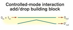
The CMI mode add/drop device is a multiplexer in the sense that it adds or drops light power from one waveguide to another. The CMI mode add/drop separates the mode interaction responsible for the loss of the device from the mode interaction responsible for the crosstalk of the device. That is due to the fact that different paths are implemented using different modes. As shown in Figure 2, the first path connects the zero-order mode of the first waveguide (denoted in the diagram by 0in) with the zero-order mode of the same waveguide 0out. The second path connects the first-order mode of the first waveguide 1in with the zero-order mode of the second waveguide 0'out.
These paths are responsible for the loss of the device. However, the device's crosstalk originates in the third path that connects the zero-order mode of the first waveguide 0in with the zero-order mode of the second waveguide 0'out. Therefore, the efficiency of the multiplexer in terms of loss is not related to its efficiency in terms of crosstalk. This factor enables the construction of mode add/drop devices with very low crosstalk that are very tolerant to the inevitable process variations. Furthermore, since the crosstalk is highly tolerant to the coupling constant and phase difference, it relaxes the requirements from the process in terms of precision and repeatability of gaps between waveguides and uniformity of other process parameters. As such, the crosstalk is orders of magnitude lower and depends very weakly on wavelength and polarization compared to DC-based devices.
The second building block of CMI switches is a dynamic mode converter device. This device operates on a multimode waveguide and has two modes of operation. In the "off" state, the mode converter acts as a passive device in which the light beam passes through the device with very little change. The mode order is not changed and the insertion loss is very low. The mode converter structure is fully symmetrical, resulting in very small wavelength dependence and allowing broadband operation. In the "on" state, the refractive index is changed by a thermo-optic effect to achieve mode conversion. In this case, the order of the mode entering the mode converter changes (usually, from the zero-order mode to the first-order mode).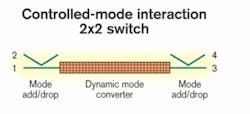

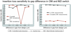
Figure 5 illustrates the difference in the dependence of the crosstalk value on variation of the waveguide gap (a critical design and process parameter for the DC). The comparison is made for equivalent single 2×2 switching units, one with an MZI design and the other with the CMI design. The crosstalk of the MZI switch is highly dependent on this gap parameter. With typical state-of-the-art process variations of ±0.5 µm in precision, the DC-based MZI switches are highly susceptible to the quality of the facilities and process. As for the CMI switch, the isolation value remains excellent even beyond ±2 µm from the intended design, which is four times larger than the typical PLC process parameter variation. As such, CMI devices are highly tolerant to process variations, allowing a high yield per wafer.
CMI devices surpass MZI devices in many important optical performance characteristics. In any given manufacturing environment, CMI devices are inherently less sensitive to manufacturing tolerances, have higher yield, and will perform better than MZI for the same process. Furthermore, CMI can be implemented in any standard PLC manufacturing environment and platform. As such, the CMI platform is well positioned to deliver on the promise of PLC solutions. By filling the market gap left by MZI-based devices, CMI is a technology that will be able to deliver high-performance parts at cost-effective prices.
Myo Ohn is vice president of marketing and business development and Dr. Ilya Vorobeichik is founder and director of technology at Optun (Santa Clara, CA).