Exact science: Automating precise engineering processes

Poor assembly yields plague terminal-device manufacturing today. Assembly yield improvement through tightly coupled automated test and assembly can reduce component costs by an order of magnitude and increase device reliability. However, automating the precise engineering processes and measurements involved in component manufacture is challenging at best.
Laser diodes, widely used in sources and amplifiers and predominantly engineered with edge-emitting indium phosphide (InP) chips, are a good example of some of the engineering challenges involved in developing precise assembly processes. The integrity of the chip attach process—especially with regard to thermal impedance and coupling efficiency—is fundamental to the performance and reliability of the entire device.
InP chip attach is a precisely engineered process consisting of four-axis alignment, placement, and profiled in situ reflow of multiple gold-tin eutectic interfaces. The bimetallic interfaces are the critical junctions that drain heat away from a laser diode, which is capable of generating extremely high-power densities—up to 10 MW/cm2. Placement accuracy of the diode relative to the submount on which it is bonded must be maintained to within ±5-micron true position radial to ensure coupling efficiency from the laser diode to the fiber.
Of the several factors influencing chip attach integrity, the critical assembly parameters include device placement, down force, slope of the heating ramp, dwell temperature, dwell time at temperature, and slope of the cooling ramp. In-process measurements test the impact of each of these factors and give precise control over those variables that affect the assembly process.
A comparison of continuous wave (CW) and pulsed light, current/voltage (LI/V) curves gives an immediate indication of chip attach quality. A more sophisticated measurement that compares the wavelength of the output light and the temperature of the substrate for various duty cycles of pulsed operation as well as CW operation can actually measure the thermal resistance of the die bond, which gives a quantitative measurement of the bond's quality. The highest yield is achieved by paying careful attention to the results of these measurements.
The operating temperature of the laser is a key factor in device reliability, since threshold current tends to rise with temperature, increasing the amount of waste heat generated. Furthermore, laser lifetime decreases as temperature increases. To optimize heat transfer, laser diodes are attached by means of a low-ohmic, high-thermal conductivity metallization in a precisely controlled place and eutectic reflow process (see Photo 1). The solder joint functions as both the electrical contact and the primary heat transfer interface between the laser diode and heat-sink. Without a robust thermal interface, increased device temperatures severely degrade light output and device longevity.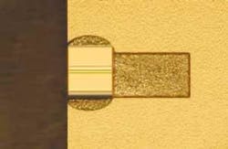
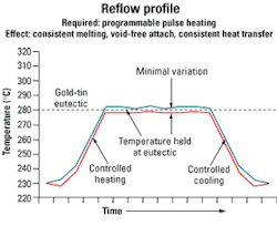
The reflow profile during an in situ eutectic die attach process is engineered to provide consistent melting and a void-free attach interface (see Figure 1). This approach results in consistent heat transfer from the laser diode and contributes significantly to temperature stabilization during laser operation. The power required to heat a device rises directly in proportion to the area required, according to the formula:
Q (heat energy required) = U (heat transfer coefficient) × A (area) × ΔT (change in temperature).
Programmable pulse heating coupled with automated component attach provides the recipe-driven process control essential to producing high-yield, high-performance laser-diode assemblies. During the in situ reflow process, temperature slopes for heating and cooling, overshoot, and dwell times are programmable to enable process optimization and repeatability. Tightly coupled temperature control ensures profiles are tracked repeatedly in production.
A basic understanding of the relative effect of the key factors in achieving reliable, low thermal impedance chip attach—device placement, down force, slope of the heating ramp, dwell temperature, dwell time at temperature, and slope of the cooling ramp—needs to be determined through a carefully designed set of experiments. These experiments provide a powerful means to achieve breakthrough improvements in product quality and process efficiency. An analysis of a variances experiment can identify the degree of contribution of each of these factors and their relative interactions. In this initial stage of process development, the appropriate design choice is a fractional two-level factorial. This type of experimental design screens a large number of factors in a minimal number of runs. During the experimental design, the following guidelines should be observed:
- Measure responses quantitatively—avoid pass/fail and subjective measurements.
- Replicate to dampen uncontrollable variation (noise), which improves the chance of detecting a statistically significant effect (the signal) in the midst of natural process variation (the noise).
- Randomize the run order to avoid influence by uncontrolled variables.
- Block out known sources of variation—divide the experimental runs into homogenous blocks, then arithmetically remove the difference, thereby increasing the sensitivity of the design of experiments.
- Know which effects (if any) will be aliased—an alias indicates that two or more things have been changed at the same time in the same way.
- Do a sequential series of experiments-execute the experiments in an iterative manner so that information learned in one experiment can be applied to the next.
- Always confirm critical findings—do a confirmation run to verify the outcome.
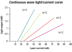
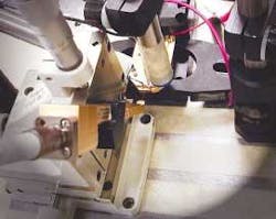
Photo 2 shows a prototype experiment designed to measure Rth. A chip-on-carrier (CoC) laser is mounted on a temperature-controlled heat-sink using a very small amount of thermal grease to maximize thermal conductivity between the carrier and heat-sink. Two probes attached to a laser-diode current controller contact the anode and cathode of the laser. Finally, an optical-fiber probe mounted on a precision five-axis alignment stage is positioned directly in front of the chip to send light to an optical spectrum analyzer (OSA).
Data is collected as follows: The laser is driven at a moderate operating current, sufficient to generate a signal that the OSA can detect but not high enough to risk damage to the laser. The laser is held at a stable temperature, Ti, typically 5° or 10°C below room temperature. The drive current is pulsed with 1-microsec pulses at a 0.1% duty cycle. Then the spectrum is measured on the OSA. For lasers with a distinct mode, such as distributed-feedback lasers, the wavelength of the main mode is measured. For lasers with many modes, such as Fabry-Perot lasers, a single mode is chosen and measured. The assumption is made here that with such short pulses and low duty cycle, the input power is miniscule and there is negligible heating. The next step is to increase the duty cycle of the drive current to 100%. With CW operation, heating at the laser can be significant, so the wavelength will change dramatically. By tuning the temperature to its final temperature, Tƒ , the wavelength of the chosen mode can be tuned back to the pulsed value. Here, the temperature, T, forward voltage, Vƒ , and drive current, I, are measured.
Taking the three measurements from the final step, Rth can be calculated as follows: The change in input power, ΔP, between the pulsed case and the CW case is simply ΔP = I × Vƒ . The change in temperature, ΔT, is the difference between the original temperature, Ti, and Tƒ . The thermal resistance is defined as the change in temperature caused by a change in input power. It is calculated as Rth = ΔT/ΔP. Typical values range from 5° to 50°C/W.
Measurements of Rth are critical in understanding how several variables such as dwell time, ramp time, and soak temperature affect the CoC die bond. In addition to getting an absolute measure of thermal resistance, a carefully constructed set of experiments can reveal the optimum assembly parameters to achieve high-integrity, consistent bond quality. Combining quantitative measurements such as Rth in a tightly coupled feedback loop with a sophisticated automated bonding process can result in significantly improved manufacturing yields and reduced component costs.
Dr. Stephen C. Bennett is a senior applications engineer at ILX Lightwave (Bozeman, MT). He can be reached at 303-516-8879 or [email protected]. Bruce W. Hueners is vice president of marketing at Palomar Technologies (Vista, CA). He can be reached at 760-931-3600 or [email protected].