Advantages of smart photonic switches in enabling all-optical networks
New all-optical switching technologies, particularly silica-on-silicon, give carriers options for eliminating costly electronics from fiber-optic networks.
Dr. Yosi Shani, Dr. Narda Ben-Horin, and Michael Leigh
Lynx Photonic Networks Inc.
Optical networks use light instead of electrical pulses for high-speed transmission of much of the world's data and voice traffic today. Implementation of DWDM in fiber-optic systems is attempting to meet the explosive demands of Internet and other telecommunications traffic. DWDM has vastly increased the amount of digital traffic that an individual optical fiber can carry, multiplexing several parallel wavelength channels on a single fiber. The number of channels per fiber increased from eight for WDM (just a few years ago) to approximately 160 for DWDM today, increasing capacity to the equivalent of several hundred thousand simultaneous voice telephone calls over a single fiber.
However, demands for still more capacity and bandwidth are becoming insatiable. The ultimate goal is an all-optical telecommunications infrastructure that promises terabit transmissions. Such an infrastructure is dependent on an all-optical alternative to the optical-electrical-optical conversion used in today's optical networks.
A key element of an all-optical infrastructure is "transparency," which enables optical crossconnects (OXCs) and remotely reconfigurable optical add/drop multiplexers (OADMs) to be data-format-, bit-rate-, and protocol-independent. Certain types of photonic switches provide such transparency.The photonic switch eliminates the need to convert light signals into electrical signals and back again to light signals. At its simplest, the photonic switch routes light signals traveling in one direction on a fiber into light signals traveling in another direction on a second fiber. The photonic switch can precisely redirect even the most complex light streams.
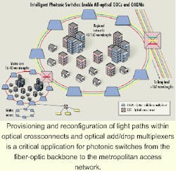
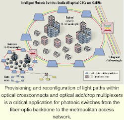
A critical application for photonic switches is in the provisioning and reconfiguration of light paths within OXCs and OADMs (see Figure 1). For these applications, submillisecond switching times optimize overall network performance. Another application is protection switching, where switches are used to switch the traffic stream from a primary fiber to a secondary fiber in the event of primary fiber failure.
Optical switches will also play an important role in high-speed optical packet-switching networks of the near future, for example, using light to switch signals on a packet-by-packet basis. For this application, the switching time must be less than the duration of a packet, specifically, a few nanoseconds.
Photonic-switch modules consist of matrices of switching elements. Each switch module is a matrix of N inputs by M outputs (where M commonly equals N in a symmetrical format).
A large array of switch elements directs the light between the N input and M output ports. These switch elements may be connected by passive waveguides, along which the light travels from one switch element to another. Waveguides are extremely thin channels etched on silicon wafers that "guide" or change the direction of light signals along curves. Each switch element in the module is connected to electrical control leads and the whole module is packaged with supporting electronics.
Several technologies can be used to construct optical switches. The popular technologies include the use of mechanical systems, bubbles, liquid crystals, holographs, and integrated optics.
- Mechanical. This technology includes micro-electromechanical systems (MEMS) that use the movement of microscopic mirrors in either two or three dimensions to reflect light to different paths. MEMS provide only basic on/off functionality and consist of moving parts. The reliability of MEMS in photonic switches is still unproven.
- Bubbles. In this technology, a small gas bubble used to reflect light is thermally created at the intersection between two waveguides. In the absence of the gas bubble, light passes unchanged through the liquid. When present, the bubble totally reflects the light to another output port. This technology involves the phase change of refractive-index-matching oil into gas and back again as well as long-term heating of the organic fluid. Bubble technology was originally developed for inkjet printing where bubbles are created within a continuous flow of a fresh fluid and therefore have essentially no effect on material stability. By contrast, a bubble switch works numerous times, using a small volume of unchanged oil, which may cause a degradation of the material and a change in its index-matching properties. In addition, the oil must be heated for long periods, sometimes several months or more, which can change the material properties as well as influence neighboring channels. As in MEMS technology, functionality is limited to on/off only.
- Liquid crystals. This method uses two basic building blocks for each switch element. First, a liquid crystal (LC) cell rotates the light polarization when voltage is applied. Second, a beam displacer serves as a polarization router, reflecting the light to one of two possible paths as determined by the LC cell. However, LC switches are limited to a very small number of ports (up to four).
- Holographs. Holographic switches can be very fast (a few hundred micro-seconds) but are limited to switching a single wavelength rather than broad-range wavelength switching.
- Integrated optics or planar lightwave circuits (PLCs). Integrated optics refers to the construction of miniaturized optical and electronic components on a common substrate such as silicon. The optical components may include arrayed wavelength gratings (AWGs), modulators, switches, filters, detectors, and sensors, all interconnected with on-chip waveguides to form integrated optical circuits that process and manipulate the lightwaves. Different ways of manipulating and controlling light signals can be used, including electro-optic, thermo-optic, acousto-optic, and magneto-optic methods. PLCs are optical circuits laid out on a silicon wafer and constructed using the tools and techniques that the semicon-ductor industry developed and fine-tuned over the last two decades. This technology enables multiple components to be fabricated and interconnected at one time, keeping manufacturing and packaging costs low. The use of integrated optics promises high functionality in the management of light-optimized performance (i.e., low loss and high extinction ratios for minimum light signal leakage) and ease of mass production. The result is compact, low-cost, and reliable optical subsystems-and the technology is stable and proven.
The silica-on-silicon (SoS) smart photonic switch uses a thermo-optic effect to perform switching. Each switch element is composed of two arms of waveguides very close together in the interaction area. By "micro-heating" one of the arms-changing its refraction index-the light is transmitted down one path rather than another. Given appropriate intelligent path control, light can be divided in any power ratio between the two paths of any switching element. Therefore, an SoS switch that employs such intelligence is not merely an on/off switch like its MEMS and bubble counterparts. Rather, it is capable of continuous output power control. An electrode connected through control electronics provides the heating.
SoS switch modules support several unique features and functions. For instance, dynamic output power control can be built into the switch module logic to manage power attenuation-a requirement that has until now only been handled outside of the switch fabric. External power control usually requires additional expensive components and complex time-consuming system integration.
Additionally, important network capabilities such as selectively weighted multicasting and broadcasting have always required a conversion from optical to electrical and back. With an SoS switch, that can be accomplished within the switch fabric to provide significant cost advantage and superior network performance. In such networks, no external power attenuators or splitters are required. This unique feature is important in many system applications and scenarios such as so-called drop and continue for inter-ring protection.
Other features include service multicasting such as for video or stock-exchange data broadcasting as well as weighted multicasting according to each path's power budget. For erbium-doped fiber amplifiers, an SoS switch enables power equalization. Software-based wavelength management can be accomplished, enabling protection restoration and provisioning that is provided at the transmission data rate on a per-wavelength basis.
Transparency, high reliability, submillisecond restoration, and nonblocking features are also inherent in the SoS switch. As these devices develop further, they will be capable of approaching switching speeds as fast as 100 microsec, a key advantage over MEMS and bubble-jet optical switches. This faster speed makes them especially suitable for restoration applications.
Ease of manufacturing is another advantage. The semiconductor industry's standard wafer manufacturing techniques enable highly reliable volume production at low cost. As a result of advances in design, architecture, and fabrication techniques, new and more efficient ways of compact design and matrix layout enable a high degree of integration on a single wafer.
In the near future, smaller and more efficient structures in integrated optical circuits will be fabricated. Researchers are exploring the fabrication of waveguides on new materials such as "contaminated" silica, in which a small concentration of other elements is added to improve light confinement. Some of the materials confine light so effectively that beams with a wavelength of 1.5 microns-the standard for telecommunications-can be contained in waveguides about a half-micron wide. These waveguides can also make turns about a thousand times tighter than the millimeter-scale bends attainable in earlier waveguides, thus enabling more condensed architectures.
Although several approaches to optical switching are promising, SoS smart switches have unique technological advantages. They also offer a high-performance, highly reliable, cost-effective solution that will enable all-optical networking to the network edge.
Dr. Yosi Shani is vice president of technology, Dr. Narda Ben-Horin is business development manager, and Michael Leigh is president and co-founder of Lynx Photonic Networks Inc. (Tel Aviv, Israel).

