PLC platform addresses emerging component requirements
This silica waveguide technology creates sophisticated functionality in small packages, which are well-suited to high-volume manufacturing.
Dr. Jerry Bautista, Dr. Kevin Sullivan, and Dr. Bob Shine
WaveSplitter Technologies Inc.
WDM has enabled capacity on fiber-based networks to increase dramatically. Initial WDM systems deployed in 1996 used four wavelength channels spaced 400 GHz apart; systems developed today offer 160 channels spaced 50 GHz apart. The success of these systems is based on the use of the inherent bandwidth of the optical fiber and deployment of optical amplifiers to reduce network costs.
While greater capacity in the long-haul backbone was the original driver for WDM systems, designs are evolving from the original point-to-point multiplexer-based systems. WDM in metropolitan networks and all-optical architectures requires more sophisticated optical components to enable intelligent, reconfigurable, mesh networks. These components include very-high-channel-count multiplexers and demultiplexers, reconfigurable add/drop multiplexers, dynamic gain equalizers, low-cost optical amplifiers, and wavelength switches. These products must meet Telcordia reliability standards and be achieved in a small package using low-cost, high-volume manufacturing techniques.
Planar lightguide circuit (PLC) technology can be used to produce components that meet many of these requirements. Components already demonstrated based on a PLC platform include 1xN power splitters, NxN star couplers, arrayed waveguide grating (AWG) routers, variable optical attenuators (VOAs), dynamic gain equalizers, waveguide amplifiers, thermo-optic switches, and channel-monitoring devices.
In a typical PLC, a silica (glass) waveguide is fabricated on either a silicon or silica substrate. The waveguide structure is produced by depositing or growing a lower cladding layer (~15-20 microns in thickness), depositing a core (~6 microns thick), defining the waveguide structure in a photolithography and etch process, and finally depositing a final or top cladding layer (~15 microns thick). Two major deposition processes are employed broadly today: chemical vapor deposition (CVD) and flame hydrolysis (FHD).The CVD approach is a modification of standard semiconductor processing. For example, the lower cladding layer can be grown from a silicon substrate wafer via atmospheric oxidation (APOX) or high-pressure oxidation (VPOX). In both cases, more than 100 wafers are loaded into deposition chambers at elevated temperature and moisture is introduced at atmospheric or elevated pressure. Processing times can vary from one day in the case of VPOX, to more than 10 days for APOX. Layer uniformity and composition are checked via monitor wafers dispersed evenly in the chambers. The core layer is deposited in other CVD reactors in which phosphorous and/or germanium are introduced in addition to silane to increase the refractive index via careful doping. Temperature profiles and chemical mass flow rates must be carefully controlled to produce uniform composition and thickness. A mask, photo-resist, and typically reactive ion etch are then employed to define the waveguide pattern. An over-etch is used to ensure complete removal of core material not required. In addition, low surface roughness and vertical walls are required for low propagation losses.
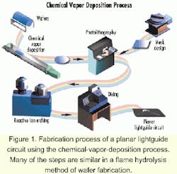
Finally, the upper cladding layer is deposited. The refractive index of the upper clad is lowered relative to the core via the incorporation of boron in addition to phosphorous. Often the upper clad is composed of several thin layers in which the viscosity of the deposited glass is gradually increased while maintaining a constant refractive index. This is done to ensure that the waveguide structure is completely covered without voids. Unfortunately, the final upper clad layer composition must also be carefully controlled to avoid combinations that are not stable in the presence of moisture. Such sensitivity to moisture causes devitrification or the formation of crystalline centers, which create severe scattering of light and can result in reliability testing failure. The production of a PLC using the CVD process is outlined schematically in Figure 1.In both the CVD and FHD processes, it is critical to carefully control the geometry and composition of the deposited layers. For example, the refractive index should be accurate to within one part in 10,000 and the thickness should be accurate to within roughly 0.2 micron of the target thickness and uniform across the wafer to within 0.01 micron. These very stringent requirements allow for predictable waveguide design rules and excellent optical performance. Unfortunately, systematic process variations occur that result in departures from ideal geometry and composition. These variations result in impairments to the predicted optical performance, and thus waveguide designs must be modified to account for these variations. Successful waveguide design often requires multiple iterations upon design and wafer fabrication. Obviously, once a successful design is selected, the deposition and photolithography processes must remain stable to avoid further design iterations.
The rather large dimensions of the resultant devices, roughly 1 cm x 3 cm for AWGs, makes it imperative that cleanroom conditions prevail to avoid incorporation of particulates. These impurities can significantly increase propagation losses, rendering entire wafers useless.
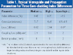
It is not clear whether CVD or FHD is the preferred deposition method. Each has strengths and weaknesses that can enable various waveguide designs to more closely meet customer requirements. The FHD technique allows a higher concentration of germanium to be doped in the core region, creating a higher index difference and allowing tighter waveguide bend radii. A tighter bend radius does allow smaller overall device sizes but at the expense of higher coupling losses due to the fiber-to-waveguide mode-size mismatch. Typical waveguide properties of medium, high, and super-high index-difference structures are illustrated in Table 1.1
While the initial WDM systems used thin-film filters to combine or separate wavelength channels, this technology is limited by poor scalability in form factor with increasing channel count and decreasing yield with denser channel spacing. Instead, AWG routers have emerged as an attractive choice for DWDM systems due to their compact size for high-channel-count systems, good optical performance characteristics, low cost per channel, and ability to scale to large volumes easily. Additional benefits include the possibility of rapid prototype design cycles and "mass customization" to meet customers' unique demands in repeatable, high-volume production.
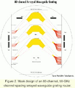
In an AWG device, an incoming signal is transmitted first through the input waveguide and then into a slab propagation region. This slab region couples the light into a large number of waveguides, which act as a phase array due to the constant path length difference between adjacent waveguides. The light then propagates into a second slab region where it is focused in a wavelength-selective manner into the output waveguides. AWGs with channel counts between eight and 40 are commercially available and have been in deployment since the mid-1990s. In the laboratory, AWGs with up to 256 channels have been demonstrated.2 An 80-channel AWG is shown in Figure 2.Important performance criteria for an AWG include both single-channel specifications as well as uniformity issues due to the large channel counts. As with any multiplexer or demultiplexer, the lowest insertion loss possible is desired. With an AWG, the insertion loss is determined by fiber waveguide coupling losses, waveguide propagation losses, and the design tradeoffs associated with the required passband width and free spectral range. A significant advantage of the AWG is that this loss does not scale linearly with channel count, allowing relatively low-loss devices to be fabricated for very high channel counts. The passband shape becomes an issue as components are cascaded together, and for this reason, a flat passband shape is often preferred to a Gaussian design, albeit with an insertion-loss penalty of ~3 dB. Some applications of Gaussian designs can still be found in metro and access deployment where insertion loss is at a premium due to a lack of amplification in the network architectures.
Crosstalk performance is an important parameter in a demultiplexer, and adjacent, nonadjacent, and total crosstalk values should be specified for the device. These values lack meaning if a wavelength window about the ITU grid is not defined across which the performance is quoted. This window width is typically defined as 30% to 50% of the channel spacing and represents a statistical view of the laser drift range for the application.
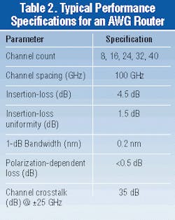
Finally, because of the large number of channels, insertion-loss uniformity is a parameter of interest. This loss uniformity is often dominated by the transmission roll-off that occurs on the order of 2-3 dB due to Brillouin zone edge effects. The insertion loss and loss uniformity can be improved by increasing the free spectral range of the device design, with a resultant increase in the chip size. Table 2 lists some typical optical performance values of commercially available AWGs.
While the AWG as described does satisfy many of the needs of next-generation optical components, mature packaging and product reliability are also key market requirements.Today's gigabit transmission rates through high-channel-count AWGs underscore the importance of device reliability. Failure modes for this class of device can include a failure of the fiber attachment joint, moisture sensitivity in the deposited glass, and mechanical failures in the piece parts used in the assembly. Manifestations of these modes span catastrophic failure to a degradation in performance associated with, for example, spectral drift or loss variation. Device reliability is critically connected to the coupled variability introduced by optical design, glass composition, dicing and polishing methods, fiber-attachment methods, and the packaging process. For example, improperly designed circuits may have acute sensitivity to bond creep, or highly doped glasses may be environmentally unstable and thus require hermetic packaging.
Some concerns were raised in the mid-1990s about the long-term reliability associated with epoxy in the optical path on the planar platform.3 This concern resulted in greater scrutiny of bonding materials and a customer perception that epoxy was a liability. This perception is generally incorrect for PLCs in that loss of adhesion is rarely encountered, even under harsh and high-power conditions (>500 mW), if the epoxy characteristics are properly chosen and the bond is not under packaged mechanical stress.
An understanding and mitigation of the failure modes through design verification leads to a robustness in the design, fabrication, and packaging of AWG devices. The reality is that high-channel-count products (>40 channels) have been fully qualified to Telcordia 1221 requirements and are in wide-scale deployment today.
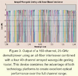
While Figure 2 demonstrates an AWG capable of demultiplexing 80 channels with 50-GHz channel spacing, this may not be enough for future DWDM systems. An alternative approach to very high channel counts is to combine the advantages of high-channel-count AWGs with dense channel interleavers.4 An example of such an approach is demonstrated in Figure 3. In this system, four 40-channel AWGs are combined using a 1x4 all-fiber interleaver to create a 160-channel demultiplexer with 25-GHz channel spacing. The temperature tuning of the individual devices allows for optimization of the system-level optical performance. This system demonstrates excellent spectral filtering properties across a wide wavelength range, with a worst-case channel offset on the order of 10 pm.
Any company considering entering this market must consider the intellectual property already developed by the established AWG players. These companies have spent millions of dollars on research and development over many years and will protect their intellectual capital. While smaller startup companies may not yet be visible to these suppliers, the potential large market capitalization makes this unlikely in the future. The choices then become: license the intellectual property if available, attempt to design around it, or limit designs to public domain intellectual property.
In addition to high-channel-count multiplexers and demultiplexers, next-generation optical networks require more sophisticated optical amplifier components. In DWDM networks with high channel counts, it is important to ensure that none of the channels become significantly weaker than the others after transmission through multiple amplifiers, or the signal-to-noise ratio will be reduced. Reconfigurable networks also create a variable load on the amplifier as the wavelengths are routed to different segments of the network, making it necessary to dynamically adjust the amplifier gain. Finally, metro networks need low-cost amplifiers with modest gain. These different functions can all be met with PLCs.
VOAs allow individual channels to be balanced to compensate for amplifier nonlinearities and avoid receiver saturation or overload. The channel power can be adjusted by varying the individual laser current; however, reducing the laser power this way changes the laser wavelength and closes down the system eye-diagram. An optomechanical switch offers another method to attenuate the signal power, but these devices tend to be bulky, slow, and may stick if left static for long periods of time. A PLC VOA can be designed to integrate multiple channel attenuators in a single, small package and is based on solid-state technology for improved reliability. Attenuation values of 20 dB, response speed on the order of 1 MHz, and low polarization-dependent loss can be achieved in PLC VOAs.
An automatic wavelength channel-by-channel equalizer has also been demonstrated for high-channel-count systems using a Mach-Zehnder interferometer and individual thermo-optic phase shifters for each lens waveguide.5 The device offered both broadband gain flattening with sufficient resolution to individually adjust over 40 wavelengths. In this device, a filter was created in one arm of the inter-ferometer using an AWG-lens-AWG combination with phase shifters in the lens region. The device acts like an interferometer for each channel, equalizing the channel power at the output using constructive or destructive interference. In this way, channels that don't require gain equalization are left alone, eliminating unnecessary attenuation.
A final amplifier product based on PLC technology is the waveguide amplifier. In this device, the waveguide structure is doped with erbium atoms using an ion exchange process, acting much like an erbium-doped fiber amplifier. The difference is that the gain medium in a waveguide amplifier is much shorter and has higher concentrations of erbium. While this creates only a modest gain value, typically ranging from 8 to 15 dB, it is adequate for the shorter span lengths in metropolitan networks. Like other PLC products, a waveguide amplifier also offers the benefits of integration with other functions. An example of this is a fully loss-compensated splitter where the amplifier is combined with a power splitter to compensate for all the losses introduced by the splitter. Other functions not normally integrated with an amplifier can now be integrated on a single chip, reducing the total footprint. The mass fabrication process reduces the manufacturing cost of the device.
While only a few specific products have been discussed, it is clear that PLC technology creates a robust, flexible technology platform for the sophisticated optical components required for next-generation optical networks. The integration of multiple functions on a single chip reduces the overall size and cost, wafer processing allows for rapid prototyping of design with scalability to very high volumes, and careful design techniques can fully satisfy Telcordia requirements. PLCs will allow intelligent optical networks to become a reality.
Dr. Jerry Bautista is chief technology officer and senior vice president of technology, Dr. Kevin Sullivan is vice president of engineering, and Dr. Bob Shine is director of marketing at WaveSplitter Technologies Inc. (Fremont, CA).
- K. Okamoto, Fundamentals of Optical Waveguides, Academic Press, New York, NY (2000), p. 343.
- Y. Hibano, et al., "Fabrication of silica-on-SI waveguide using higher index difference and its application to 256 channel arrayed-waveguide multi/demultiplexer," presented at OFC (March 7-10, 2000), Paper WH2.
- S. Eternad, et al., "A Failure Mechanism for Optical Power Branching Components," presented at NFOEC (June 18-22, 1995).
- B. Shine and J. Bautista, "Interleavers make high-channel-count systems economical," Lightwave, August 2000, p. 140.
- C. R. Doerr, et al., "Automatic wavelength channel-by-channel equalizer," presented at OFC (March 7-10, 2000), Paper PD20.
