New photonic-switching technology for all-optical networks
Andrew Ware Agilent Technologies
Explosive information transmission from sources such as e-commerce and digital music/video distribution is generating enormous capacity requirements for telecommunications service providers. Experts predict the network backbone in 2003 will require 36 times the capacity of 1995.
New technologies have emerged to ameliorate this bottleneck by increasing the capacity of fiber. Dense wavelength-division multiplexing (DWDM) increases the capacity of fiber by multiplexing several parallel wavelength channels on a single fiber. Data rates on single wavelength channels are increasing to 40-Gbit/sec line-rate interfaces. Many of these high-speed interfaces can run different protocols such as Synchronous Optical Network/Synchronous Digital Hierarchy (SONET/ SDH) or Internet protocol (IP).
As capacity demands escalate, service providers face competitive pressure to deliver it at the lowest cost per bit per kilometer, rapidly provision new services, and reconfigure bandwidth to meet customer requirements. Current optical-to-electrical-to-optical (OEO) techniques will have difficulty meeting the needs of this new network, however. At these high data rates, optoelectronics are expensive. Switching electrically at 10 and 40 Gbits/sec is difficult enough; a network environment with multiple protocols operating at different speeds compounds the problem.
In the future, many network functions will take place in the emerging optical layer. These functions will require all-optical-network elements such as wavelength, bit-rate, and protocol-independent optical crossconnects (OXCs); remotely reconfigurable optical add/drop multiplexers (OADMs); and optical-protection switches. These elements, in conjunction with DWDM, and faster line rates, promise to revolutionize communications networks.
All-optical-network elements will eliminate bottlenecks and create more service delivery options. For example, telecommunications service providers will be able to offer "leased" wavelength services, where an entire wavelength channel is dynamically provisioned to the user. Potentially, thousands of these wavelengths could be routed desktop to desktop. All-optical elements will also eliminate costly OEO conversions (and bottlenecks); some analysts have forecast savings as high as 75%. Optical equipment can further reduce operations costs by simplifying the network, enabling a single IP layer to operate directly over the optical layer. All-optical devices will also be futureproof, allowing providers to incorporate higher line rates, new protocols, and additional wavelengths without costly upgrades.
The core technology of these optical-network elements is all-optical switching. This compact all-optical matrix switch does not require complex feedback control systems. Two well-established technologies-silica planar lightwave circuits (PLCs) and thermal inkjet technology-combine to create the basic-switch building block. (Hewlett-Packard has shipped 100 million inkjet-based printers.) The result is a reliable, low-cost solution, which is scalable to higher-order NxN switch architectures.
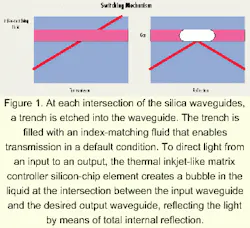
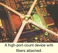
The switching mechanism consists of intersecting silica waveguides. At each intersection, a trench is etched into the waveguide. The trenches are filled with an index-matching fluid that enables transmission in a default condition. To direct light, the thermal inkjet-like matrix-controller silicon-chip element creates a bubble in the liquid at the intersection between the input waveguide and the desired output waveguide, reflecting the light by means of total internal reflection (see Figure 1). A complete integrated device with fibers attached to all ports is shown in the photo on page 98.Because of its switching mechanism and device construction, this subsystem meets the following key optical-switching performance specifications:
The switch fulfills the sub-10-msec switching requirement and achieves high port count with low loss (typical worst path fiber-to-fiber loss of 7.5 dB is obtained in a 32x32 switch). There are no polarization, wavelength, or bit-rate dependencies, and crosstalk has been measured at <-50 dB.
This technology also allows volume manufacturing, achieves high yields, and functions in the context of a larger telecommunications system. Packaging and fiber attach are key issues in achieving these goals. With other all-optical technology approaches, packaging and fiber attach present a problem. For this all-optical switch, however, the fiber is attached to all ports using a standard process. The PLC technology is promising in terms of volume manufacturing and offers the associated cost efficiencies. All measured specifications and volume manufacturing requirements have been considered in the context of a packaged solution, which includes fiber connections.
Reliability is extremely important for the applications where optical switching is used, given that terabits per second will flow through the device. The switch must meet stringent environmental requirements for temperature variations, vibration, and humidity. It also must operate for many years without failure, switch states several times over its lifetime, and operate dependably after it has been idle in a specific state for a lengthy period.
In this device, the inkjet-like matrix elements have been switched on and off millions of times without problems. An index-matching liquid is used that is inert (noncorrosive) and stable over tens of years of expected operation. Given that the device has no moving parts, the switch is expected to have the superior reliability required for telecommunications applications.
Two additional waveguides are included in the system-a redundant switching path and test path. The redundant path can be switched to in case of a failure at any switching point. The test path includes a laser and detector that continuously monitor the health of the system. This additional functionality enhances the reliability and serviceability of the switch-key criteria for switch selection beyond bare optical specifications.
In optical-crossconnect applications, it is important that the optical switch is scalable to larger NxN architectures. This technology provides scalability to large, multistage NxN architectures.
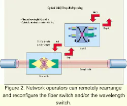
In a long fiber span, or on a ring, usually 20% to 30% of the wavelengths are dropped off at intermediate nodes. An OADM can add and drop wavelengths while enabling express channels to pass through the device untouched. This optical subsystem can serve as the switching technology for an OADM that supports remote reconfiguration and rearrangement, which allows the device to drop any wavelength to any port without manual intervention (see Figure 2).In the Figure 2 implementation, several fibers of a bundle are switched using a "fiber switch" to a second wavelength switch. The second switch is used to add and drop wavelengths to and from their proper destinations. The optical subsystem can switch any wavelength to any output port and can switch fibers or wavelengths equally well. This functionality gives the OADM flexibility, a requirement for dynamic networks that is especially important within the metropolitan area. Fixed add/drop multiplexers that incorporate fixed circulator/ grating technology do not offer the same level of remote reconfiguration.
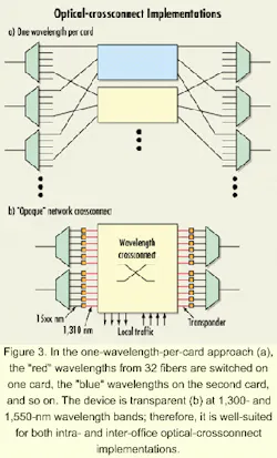
Another basic switching application is the OXC. The optical subsystem employed to create the OXC should scale to larger NxNs and be nonblocking in all configurations. These devices can be intra- or inter-office in nature.There are several ways to implement a larger crossconnect. Figure 3a illustrates a "one-wavelength-per-card" approach. If (N) is the number of fiber and (M) the number of wavelengths, a single-stage architecture requires M NxN switches. Thus, the "red" wavelengths from N fibers are switched on one card, the "blue" wavelengths on the second card, and so on.
The switch subsystem can also construct large N*M OXCs through multistage architectures such as Clos. The natural scalability of the device enables these higher-level architectures. Figure 3b shows an OXC in an all-optical core-network implementation. The device is transparent at the 1,300- and 1,550-nm wavelength bands; therefore, it is well suited for both inter- and intra-office OXC imple men tations.
A failure such as a fiber cut can create havoc for a service provider. Typically, 50 ms are allotted to the network for the protection-switching application. Of this total, only a few milliseconds are given to the optical switch.The device must switch wavelengths or fibers equally well. This functionality in addition to the sub-10-millisecond speed of the described optical switch makes the technology well suited for protection-switching applications. Protection switching can also be combined with the OXC or OADM functions.
The waveguide technology has shown the potential to scale to high port counts. Other compact waveguide geometries can be manufactured, such as multiple 8x8 switches or 1x2 switches in a single waveguide package. Optical components could also be combined with the optical switch. These components could include variable optical attenuators, gain elements, and arrayed waveguide grating multiplexers/ demultiplexers. It is even conceivable to create an OADM on a single chip.
As the all-optical layer becomes more dominant, OXCs, OADMs, and optical protection switches will be at the heart of every next-generation telecommunications network. An all-optical switch is the enabling technology for these network elements. The optical properties, reliability, port density, cost, and future potential of this optical-switch technology position it as a enabling technology for the all-optical network layer for many years to come.
Andrew Ware is an optical-networking product marketing manager at Agilent Technologies (Santa Clara, CA). Ware can be reached at andrew_ware@ agilent.com.


