Autocloning delivers photonic-crystal components
Photonic crystals (PCs) are multidimensional periodic structures with a period of submicron scale. They are promising materials for developing unique optical functions and achieving efficient integration. By choosing structural parameters such as constituent materials, types of symmetry, and their period, PCs can be freely designed with such fascinating properties as light localization, dispersion, and anisotropy. PCs have been eagerly studied for the last decade; however, no PC-based components or devices have been produced commercially yet (except photonic-crystal fibers) due to the difficulty in fabricating periodic nano-structures.
A new method of fabrication, called "autocloning technology," has shown its feasibility for commercializing PCs.1 The technology has much potential to provide a number of unique components and devices for optical communications. An ultra-thin polarizing beamsplitter is the first component manufactured via this technique to reach the market (see accompanying sidebar, "Ultra-thin polarizing beamsplitter").
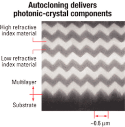
Autocloning is a key technology for producing photonic crystals having periodicity in the normal direction to the substrate. The process begins with the formation of a periodic corrugation pattern on a substrate by electron-beam lithography or photolithography. Two kinds of dielectric films are then stacked alternately on a substrate by an appropriate combination of sputtering deposition and sputter etching. Under appropriate conditions, the deposition of the multilayer progresses along with the preservation of the surface corrugation pattern. In this way, a two-dimensional periodic structure can be formed simply and sequentially.Figure 1 shows a cross-sectional scanning-electron-microscope (SEM) photograph of the autocloned PCs. For use as a polarizing splitter for the optical communications region, silicon (Si) and silicon dioxide (SiO2) are the best choices because of the high contrast of their refractive indices, and they have no absorption. During the stacking process, the surface shape automatically evolves into a triangular wavy shape in spite of the rectangular pattern formed on the substrate. That shows the surface shape is determined by the process conditions and is stable against disturbances. As a result, this method is reproducible, reliable, and suitable for industrial production. Following are some applications of PC polarizing splitters.
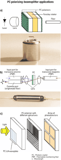
Optical isolator. Polarization-dependent optical isolators are essential for stable operation of laser modules. Cost-effective isolators for transceivers are strongly required in access and metro networks. Figure 2a includes a schematic drawing of an isolator composed of two PC polarizers attached to a Faraday rotator giving 45-degree polarization rotation. A light radiated from a laser transmits through the isolator and couples to a fiber. As for light propagating backward, one polarization is reflected on the splitter and the other is shifted by multireflection between the splitters and focused out of the laser diode.
This type of isolator does not absorb light, which leads to robustness for high optical power. To date, a prototype of the isolator was assembled and characterized. An isolation of more than 40 dB and insertion loss <0.3 dB were attained at the wavelength of 1550 nm, which shows the device's performance is sufficient for practical use.
As an ultra-thin isolator featuring monolithic integration of polarizers on both sides of a Faraday rotator has been developed. The isolator will be the ultimate isolator offering assembly-free, resin-free configuration and high reliability.
Polarization-beam combiner. Raman amplifiers, which provide optical gain in a wide wavelength region, need polarization multiplexing to obtain higher pumping power. Conventional polarization-beam combiners (PBCs) consist of a birefringent crystal. They need precise polishing, which makes it difficult to reduce their assembly cost. Figure 2b shows a new configuration for a PBC by using a PC polarizing beamsplitter.
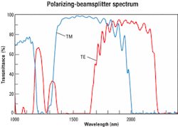
When orthogonally polarized waves from the two polarization-maintaining fibers (PMFs) are projected into the PC, the transverse magnetic (TM) wave, whose electric field is perpendicular to the grooves, transmits through it, and the transverse electric (TE) wave, whose electric field is parallel to the grooves, is reflected by it; then they are coupled into the common port of a singlemode fiber. There is no need to polish this splitter. By using the PC splitter and a twin-hole ferrule, alignment becomes much simpler and the device can be made more compact and cost-effective than existing devices. A sample of such a PBC is shown in the Figure 2b photo. Insertion loss <0.6 dB, extinction ratio >20 dB, and return loss >50 dB were obtained by using the PBC. This optical performance is comparable to that of existing devices. Several reliability tests such as robustness for high power (2 W) and the damp heat test have been passed.
Polarization state monitor. Polarization-mode dispersion (PMD) compensation devices and related components are being developed for a future 40-Gbit/sec system. A polarization state monitor is one of the important components for such a system. Autocloning technology can also be used to provide it.Arbitrarily arranging an optical axis is another unique use of PC polarizers. Figure 2c shows polarizers having three sections with different optical axis orientations. To fabricate the PC polarizers, sections of line-and-space patterns with an orientation of 0, 45, and 90 degrees are formed on a substrate, then a multilayer is deposited by a sequential autocloning process. Waveplates can also be formed using an autocloned PC designed as a birefringent plate.2 By attaching the polarizer and a quarter-wave plate to an array of photodetectors, a simple polarization state monitor can be constructed.
Another important application of PCs is for planar photonic circuits. Autocloning can also be adapted to that, because of the "heterostructure" of photonic crystals.3 To fabricate this circuit, a mulitlayer is deposited by means of autocloning on a substrate with a number of blocks having different corrugation patterns. Each block can be designed independently to show passband or stopband. Therefore, wiring waveguides and functional blocks such as distributed-Bragg-reflector (DBR) mirrors, superprisms, and dispersion compensators can be integrated.
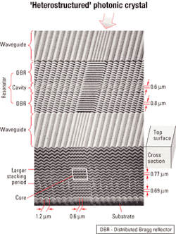
Recent research and development of PC-based waveguide devices has resulted in a functional chip consisting of two waveguides sandwiching a resonator (see Figure 3), representing the second stage of autocloning technology.For practical use of photonic-crystal chips, there are two requirements: efficient coupling with I/O fibers and low propagation loss. As to coupling to fibers, butt-jointing is much more advantageous than lens coupling. The PC waveguide was designed to have a mode-field diameter of approximately 4 mm, which can be matched to currently available high-D fibers. Propagation loss as low as 0.23 dB was recently attained.4
The fabricated sample in Figure 3 was butt-jointed with two high-D optical fibers. In the device's transmission spectrum, a sharp resonance peak was observed in the middle of the stopband extending from 1.44 to 1.53 mm. The quality factor Q was 270.
The resonant peak wavelength and the Q-factor are designed arbitrarily based on the cavity length and the number of the cells for a DBR. The concept of heterostructures exemplified by waveguides and resonators can be extended much further. Just by patterning a substrate and stacking layers, it's possible to achieve circuit functions such as DBR mirrors, corner reflectors, resonators, superprisms, delay compensators, and lenses.
Autocloned PCs can be adapted to suit a broad range of optical applications. The PC polarizer/polarizing beamsplitter meets several requirements for industrial use, including stable a manufacturing process and high performance. Its unique optical path configuration enables several novel device structures. To our knowledge, PC polarization splitters are the first photonic-crystal chip to appear on the market. The application to inplane light propagation promises to provide integrated functional chips for prospective optical systems.
Shojiro Kawakami is co-founder and president of Photonic Lattice Inc. (Sendai, Japan) and professor of NICHe at Tohoku University. Wataru Ishikawa, Takashi Sato, and Takayuki Kawashima are researchers at the company. They can be reached via the company's Website, www.photonic-lattice.com.
- S. Kawakami, Electronics Letter, Vol. 33, No. 14, pp. 1260-1261, July 3, 1997.
- T. Sato et al., Optical and Quantum Electronics, Vol. 34, No. 1, pp. 63-70, December 2001.
- S. Kawakami et al., "Active and Passive Optical Components for WDM Communications II," Vol. 4870, pp. 279-288, Proceedings of SPIE, July 2002.
- Y. Ohtera et al., "Fabrication and characterization of low loss heterostructured photonic-crystal waveguides," OFC 2003, ThI6, Atlanta, March 2003.
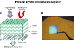
The polarizing beamsplitter (AUTOPOL), shown in Figure 1*, consists of a dielectric multilayer with a triangular wavy corrugation formed on a patterned substrate. It separates two orthogonal polarized beams by means of transmission and reflectance and thus can act as a polarizer as well as a polarizing beamsplitter. The overall layer is as thin as several microns; therefore, the component is an ultra-thin polarizing beamsplitter. Its operation originates from the polarization dependence of the Bragg reflection range; that is, the transverse magnetic (TM) wave is in a passband and transverse electric (TE) wave is in a stopband, due to the form-birefringence. In addition to its small thickness, the features of the component are as follows:
- The device is planar and therefore can be treated as a mirror.
- A device having a uniform large area (e.g., 20 mm square) can be obtained.
- Excellent characteristics (low insertion loss and high extinction ratio) are achieved.
- Various materials such as a Faraday rotator can be used for the substrate.
- .The device can be designed with a high degree of freedom, because the optical axis and operating wavelength can be controlled by adjusting the substrate pattern. This feature makes possible selecting an operating wavelength from 2 mm to the visible/ultraviolet range.
- The sputtering process is well established, thereby offering prospects for high productivity.
*Y. Ohtera et al., Electronics Letter, Vol. 35, No. 15, pp. 1271-1272, July 1999. Also, T. Kawashima et al., OFC 2003, ThI2, Atlanta, March 2003.

