Wide temperature lasers offer promise for high-speed applications
by Matt Traverso
The proliferation of high-speed data communications and high-definition video is driving the need for higher-speed interfaces nearer to the edge of the network. Network edge applications such as wireless backhaul, data center backbone, and FTTX aggregation are all focusing on higher data rates to mitigate traffic congestion. These edge applications are physically more challenging for high-data-rate and longer-reach applications than traditional telco infrastructure.
As the wireless industry works on deploying 3G and laying the groundwork for 4G, many experts have looked to optics to perform wireless aggregation. Many wireless aggregation applications operate in uncontrolled environmental conditions. Meanwhile the energy cost of communications infrastructure is rising. According to a McKinsey study (http://uptimeinstitute.org/content/view/168/57), "Data center electricity consumption is almost 0.5% of world production." Additionally, FTTX applications are being more widely deployed. In North America, Verizon's FIOS program has been successful, and the company is studying to expand their installation plan, according to Verizon CFO Doreen Toben (http://telephonyonline/access/news/verizon-rural-wireless-0529/.
These high-speed network edge applications all benefit from optical interfaces with wide temperature performance.
Over the past decade great progress has been made in the fabrication of semiconductor lasers with such wide temperature operating range. There are three primary thermal ranges that manufacturers target: semicooled operation in a Network Equipment Building System (NEBS) environment; uncooled operation in a NEBS environment; and industrial temperature range. The NEBS temperature range for the optical interfaces is defined by both the thermal environment of the building as well as the thermal rise within the communications equipment. Traditionally, this has meant that optical module case temperatures should range from 0° to 70°C for controlled applications, and �40° to 85°C for uncontrolled environments.
Semicooled operation of the laser is typically defined to mean that the laser temperature is constrained to operate over a narrower temperature window than that specified for the optical interface on the equipment. Semicooled light sources still require a thermoelectric cooler (TEC) to ensure that the laser does not exit its operating range, but the TEC need only consume power at very high or very low temperatures. This enables the optical interface to consume less power, reducing the energy cost of the equipment.
Uncooled lasers are simply wide temperature lasers. The wide temperature range is designed to exceed the span of the environmental operating conditions of the communications equipment in which they're used. For example, to meet an optical module maximum case temperature specification range, the laser should exceed all required specifications for 5° to 10°C below the minimum module temperature and 15°C above the maximum case temperature. Optical component and module manufacturers focus engineering effort on the design and fabrication of good thermal channels to minimize the extra thermal range required by the laser.
The so-called industrial temperature range is usually specified for outdoor applications such as base stations or neighborhood premises equipment. Outdoor applications have thermal operating ranges that span from high-altitude cold climates to hot and dusty regions at the edge of deserts. Component manufacturers design the laser to work in a completely uncooled fashion, but initially some applications may be built with semicooled lasers. In such instances, a standard uncooled laser may be used but in a semicooled package. During operation, the TEC is used to heat the laser when the temperature is colder than the laser can tolerate and is used as a cooler when the environment grows too hot.
There are a number of motivations for laser designers to focus upon wide temperature range operation. First, uncooled lasers enable lower-cost packaging. An uncooled laser package removes many items: the TEC that provides cooling; the thermistor that determines the laser temperature at any point in time; and the thermal control loop. Additionally, the package itself may be composed of lower-cost materials in a more manufacturing friendly outline. For example, the 10-Gbit/sec lasers used in XFP and SFP+ are packaged in TO cans. This is a cylindrical package that has been used in high volume for transistors, CD-ROM lasers, and DVD lasers.
Second, a wide temperature range increases the yield of lasers for WDM applications. Since a laser's emitted wavelength depends upon the temperature, a laser that operates over a wide temperature range can be thermally shifted to occupy an adjacent WDM channel.
In the 2002 timeframe, Opnext began manufacturing DFB lasers operating at 10 Gbits/sec that could operate over a wide enough temperature range that the laser could be uncooled; others have more recently followed suit. VCSELs for the various Ethernet and Fibre Channel data rates of 1, 2, 4, 8, and 10 Gbits/sec have been able to operate uncooled since their introduction into the marketplace. However, for longer reaches at 10 Gbits/sec as well as for moderate reaches at higher speeds more robust optical transmission sources are required.
Advances in materials growth techniques are leading toward electroabsorption DFBs (EA-DFBs, sometimes called externally modulated lasers, or EMLs) with wide temperature operating ranges to meet such requirements. These new lasers can be operated without a cooler to save costs, simplify packaging, and reduce power consumption. Laser manufacturers have been working to develop these lasers for 10, 25, and 40 Gbits/sec to meet these high-speed network edge applications.
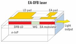
As depicted in Fig. 1, the EA-DFB comprises two sections: a DFB operating as a continuous-wave light source, and an EA modulator that acts as a shutter to turn the light on and off. Electroabsorption is the application of the quantum confined Stark effect where an applied electric field shifts the band edge of a material, thus changing the absorption properties of the waveguide.
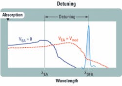
The DFB portion of the chip emits light at a wavelength, ¿0, which is a function of the DFB grating as well as the gain window of the multi-quantum well (MQW) active region of the laser. The EA modulator region of the chip operates as a band edge phenomenon—the absorption edge is located at a particular wavelength, which is a function of both temperature and bias voltage.
Materials engineering is critical to best control the behavior of the EA modulator and DFB sections of the laser across temperature and bias voltage. The DFB section and EA section are both composed of MQW waveguides. Traditionally, the InGaAsP material system has been used for semiconductor lasers in the communications wavelength windows. Recently, manufacturers have begun using InGaAlAs, which has better confinement of electrons (negative charge carriers) and smoother injection and extraction of the holes (positive charge carriers). These material properties enable higher output power, greater slope efficiency, and more stable performance over temperature.Three factors explain why EA-DFB lasers are used for higher speed and longer reach applications than directly modulated lasers: extinction ratio, rise and fall time, and constrained chirp.
In optical communications, extinction ratio is the power ratio of power used to transmit a "1" level (P1) to the power used to transmit the "0" level (P0):Finally, chirp (also known as the alpha parameter) is a measure of the shift in transmitted wavelength as the light source is modulated. A typical directly modulated laser such as a DFB is positively chirped with an alpha parameter value of about 2 to 6. Since an EA-DFB is externally modulated, the alpha parameter is constrained to values between â��1 to +1. A chirp value of zero indicates that there is no wavelength or linewidth shift as the light is modulated—this is the desirable case for optical transmission. When the wavelength shifts as the light is modulated, the chromatic dispersion of the optical fiber spreads out the optical pulse and can smear the difference between a "1" and "0" level in time, thus causing errors.
As mentioned earlier and shown in Fig. 2, an EA-DFB has some wavelength dependence. An EA-DFB is one of the most commonly deployed instances of photonic integration. The two sections exhibit different wavelength characteristics. The DFB section wavelength drifts over temperature at a rate of about 0.1 nm/°C. The EA modulator section wavelength edge drifts at a rate of about 0.7 nm/°C, for a differential drift of 0.6 nm/°C. This differential drift can be problematic over a wide temperature range. The shape of the EA band edge and the wavelength separation, also known as detuning, between the DFB wavelength and the EA edge partially defines the signal transmission quality of the diode.Despite such challenges, researchers have developed wide temperature EA-DFB technology. One design approach is based upon manipulation of the voltage bias across the EA modulator section.1 The EA voltage bias is adjusted to provide a constant detuning between the EA band edge and DFB wavelength. The EA modulator exhibits good transmission characteristics when the detuning parameter is optimized. Other approaches have also been pursued.2
The 10-Gbit/sec wide temperature EA-DFBs are being deployed in XFP and SFP+ form factors. The laser operates without a TEC, so cost and power consumption are minimized. This enables module manufacturers to meet the challenging thermal and economic targets necessary in modern data centers and edge network aggregation applications.
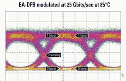
Recently, 25-Gbit/sec wide temperature EA-DFBs have been demonstrated for use in 100-Gbit/sec Ethernet applications. An eye diagram from the live demonstration is shown in Fig. 3. (Also see a video of the 25-Gbit/sec wide temperature EA-DFB demonstration on the Lightwave Channel at http://lw.pennnet.com/video/in dex.cfm under the "More from OFC/NFOEC" tab.) The IEEE P802.3ba task force has adopted a 4�25-Gbit/sec transmitter architecture centered within the 1,310-nm window with about 8-nm wavelength pitch between channels. Development of a wide temperature EA-DFB for this application enables high yield throughout the WDM channels. Additionally, by using wide temperature EA-DFBs, a semicooled architecture can be adopted to reduce the power consumption of the module. For 40-Gbit/sec applications, a fully uncooled EA modulator has been demonstrated.3
Wide-temperature EA-DFB technology is a good candidate for high-speed optical communications as high bandwidth applications approach the edge of the network. The reduced energy cost and the smaller and lower-cost packaging that wide temperature laser technology enables will help smooth the adoption of high-speed technology throughout the network.
Matt Traverso is senior technical marketing manager at Opnext Inc. (www.opnext.com).
1. S. Makino et al., "1,550-nm Uncooled EA-modulator and EA/DFB for 10/40-Gbit/s Low-power-consumption Transceivers," Lasers and Electro-Optics Society 2005, 22-28, pp. 349�350, Oct. 2005.
2. M.R. Gokhale et al., "Uncooled, 10 Gb/s 1310 nm Electroabsorption Modulated Laser," Proc. OFC 2003, Vol. 3, pp. PD42�P1-3, March 2003.
3. H. Arimoto, J. Shimizu, M. Shirai, and M. Aoki, "Wide Temperature Range, from 0 to 85°C, Operation of a 1550nm, 40 Gbit/s InGaAlAs Electro-absorption Optical Modulator," Electronics Letters, Vol. 41, Issue 1, pp. 35�37, January 2005.


