Internally compensated digital VOA modules improve cost
by Xinzhong Wang and Yao Li
OVERVIEWThe need to increase integration and standardize interfaces pertains to a variety of modules, including variable optical attenuators (VOAs). New technology can make a modular, digital VOA device design possible.Lightwave communications applications are evolving rapidly toward increased agility and flexibility. The emerging era requires deployment of reconfigurable optical add/drop multiplexing (ROADM) nodes using more standard-interfaced components. This trend pressures traditional optical component manufacturers to increase integration and create, for example, more modular variable optical attenuator (VOA) modules that can offer interchangeable digital interface capabilities directly.
To a large extent, active optical component makers forged this path earlier, transforming themselves from providers of analog lasers to producers of a variety of digitally controlled transmitters in SFP, XFP, and other standardized form factors. One key advantage of such integration toward industry-standardized modules is that it allows multisource agreements (MSAs) to be established to help sustain competition among various supporting technologies and thus promote continuous cost-improvement efforts into the future.
Although this trend has not been fully established in markets other than transmitters, it is possible that for components such as electrically controlled VOAs, the push for a modular and digitally interfaced product can result in breakthrough cost improvements and enhanced manufacturing freedom.
In today's VOA marketplace, various devices offer distinctive features in optical, electrical, and environmental performances and requirements. Each class has its own unique form factors as well. One common attribute among all is that they require analog electrical signals to drive voltage, current, or both. Yet one device design, highly favored by one system integrator, may prove to be too costly to implement for another due to the need to redesign a printed circuit board (PCB) to power the VOA engine.
From the long-term view of all system integrators, a potentially MSA-capable digitally controlled VOA module would be ideal. To promote the long-term viability of a common footprint/interface design, it would help if various enabling technologies can support it and compete at the same time.
Next-generation VOA modules must accommodate a set of commonly shared optical and electrical performance specifications. Extremes in requirements for response time, power consumption, and form factors should remain niche and be generally excluded for the broader market's common requirements.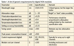
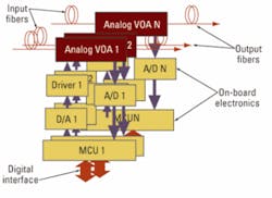
Based on our survey of various system integration applications and available technological options, a typical N-channel digital VOA module architecture is depicted in Figure 1. A set of basic requirements that balance among most application needs is presented in Table 1. Included in the requirements is also a nominal target cost per VOA channel (even in single-channel modules) that can actualize and motivate its wider application and adoption in the future.
To support a digital and modular integration approach, several common device technologies can be considered:
- electro-optic (E-O)
- micro-opto-mechanical system (MOMS)
- micro-electro-mechanical system (MEMS).
The E-O technologies have the advantage of no moving parts and possess very high attenuation tuning speed. Some of them in the planar waveguide circuit (PLC) forms are multichannel oriented with small device form factors. However, these PLC-based devices are often less competitive in some optical performance characteristics such as polarization-dependent loss (PDL), wavelength-dependent loss (WDL), and temperature-dependent loss (TDL). While the technology can address larger array VOA applications with cost reaching below $100/channel, for smaller channel counts they are less cost competitive and do not offer common drive requirements as devices.
The technologies supporting MOMS VOA modules have the longest field exposure. This type of device's actuation speed is typically slower and it is bulkier in packaging. But these devices are very reliable and can serve applications where speed, power consumption, device dimension, and thus large-channel-count array integration are not among the most important considerations. However, many MOMS VOA devices are not cost competitive due to use of more expensive and hard-to-manufacture special optical components, such as variable neutral density (ND) filters.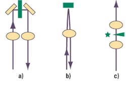
Last but not least, MEMS technology is a special class that distinguished itself from MOMS for its unique device characteristics associated with semiconductor fabrication processes. Although possessing moving parts, the small scale of a MEMS VOA chipset enables fast response time at a much smaller power dissipation level than a MOMS-based device.
MEMS VOAs have significantly penetrated the market over the last 10 years. Some may recall that during the last telecom bubble, headlines proclaimed the near availability of sub-$100 MEMS VOA devices, owing to the many desirable characteristics that MEMS manufacturing platforms uniquely possessed. Various optical MEMS foundry services were set up and so were many MEMS VOA assembly lines.
However, history proved that the sub-$100 VOA cost milestone was tough to achieve. Among the problems in improving the cost-reduction curve for MEMS was packaging manufacturing yield. Many heavily promoted advantages associated with the performance excellence and uniformity at the MEMS chip level could not overcome the dominant manual assembly processes that led to an overall lower yield at the final product level.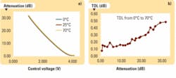
While fully automated assembly lines might have solved such assembly issues over the long term, the industry's capital limitations over the past decade would not allow component manufacturers to justify the level of investment required. In fact, without the huge volume that only the semiconductor industry can create, it may not be possible to justify the high costs of a new assembly line featuring state-of-the-art equipment and automated batch processing for the VOA application. The industry must adjust to a supply model where a more modest product volume will demand new, low-cost component technologies that require lower initial capital investment and low-cost labor support, among other considerations.
Interestingly, migration to a more standard integrated digital VOA module may also pave the way for lower total cost per channel on an industry-wide basis, based on the industry served—i.e., moderate volume, high-performance optical communications. Higher performance at lower cost per channel is a win-win for system designers. And potentially standardizing the interface enables a wider supplier base over time to please manufacturing and procurement.
To achieve the required high manufacturing yield and low component cost—without high up-front investment or requiring consumer semiconductor volumes—requires thinking about what's “in the box.” The key enabling technologies for a sustainable sub-$100 digital VOA module design might come from the innovative use of various existing, low-cost, reliable optical elements that other industries have developed and matured over recent years. Integration and packaging of commoditized components derived from these technologies must fit low-cost manual assembly platforms. Once these two most important conditions are satisfied, use of these commodity components, some of which are being manufactured in volumes exceeding 100 million pieces per year, will contribute to high manufacturing yields and propel future continuous cost-cutting initiatives as well.
Figure 2 shows a simplistic view of several technologies that can serve digital VOA module needs. These include a traditional MOMS VOA, the popular MEMS VOA, and a newer MOMS VOA featured in an internally compensated VOA (iC-VOA) module. The iC-VOA combines some of the better characteristics from traditional MOMS and MEMS technologies, and adds performance enhancements through an internal compensation scheme that uniquely fits MOMS packaging dimensions and digital module integration requirements.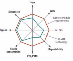
For example, what makes the MEMS VOA so sensitive to the environment (thus causing yield loss due to degrading TDL, WDL, and PDL performance) is a weakness in the MEMS's beam blocking actuation stability. The iC-VOA solves this issue with a patent-pending internal compensation technique using low-cost digital control electronics that a digital VOA module requires as well, thereby leveraging a synergy of requirements.
iC-VOA technology is low in cost due to its inherent use of commodity-volume optical elements from well-developed industries outside of telecom. It also avoids the use of an improper mix of semiconductor fab-yielded chipsets with a very high degree of sensitivity. However, at the digital module level, MEMS or E-O technologies can also satisfy the footprint and interface requirements. This compatibility increases competition and innovation from all technologies and enables multiple component sources—even if some are lower cost at the outset.
A typical iC-VOA engine's attenuation scans in the range of 0.5 to 30 dB are plotted in Figure 3 in three temperatures, 0°C, 25°C, and 70°C. Figure 3a shows the three attenuation curves. Figure 3b plots the details of the TDL, which is defined as the difference between the maximum and minimum attenuations at any set point among the three curves. The internal compensation enables a much more contained TDL performance at the high attenuation range that often caused MEMS VOAs to have low yield.
One major advantage of the internal compensation over its external compensation counterparts, such as a technique that uses a tap coupler and a photodetector in a closed-loop control, is that it achieves the same purpose with perhaps 1/10 of its enabling component cost. As for the long-term reliability concerns of the iC-VOA, the technology recently completed successfully the Telcordia GR-1221 reliability tests, thereby proving performance and reliability levels in compliance to those required by the telecom component industry.
Figure 4 shows a set of spider graphs to help properly position the IC-VOA in the emerging generic digital VOA module technology arena. Represented as the line enclosing a unity dimensional circle is a set of eight of the most important performance parameters that any generic digital VOA module would need. The other closed circle with unequal strength projection onto the same eight dimensions represents the iC-VOA's competitive positions in a qualitative view. The closer to the origin a specific dimensional projection, the more competitive that technology is.
We can see that out of the eight most important attributes the module should possess, the iC-VOA's performance meets all the requirements, with five of them (WDL, PDL, TDL, IL, and repeatability) leading. These optical performance attributes are becoming increasingly important as dynamic optical networking penetrates deeper into the fiber-to-the-home (FTTH) and broadband domains, with wavelength range requirements of typically 1260 to 1620 nm and temperature range requirements of �40°C to 85°C. The iC-VOA-based product can achieve sustainable sub-$100/channel cost for a complete digital VOA module from its launch, and it has just started its assembly cost-reduction curve.
The impact of the digital VOA module to the industry can potentially be huge as long as the cost incentive can serve as a major enabler. The digital format enables designers to extend the VOA applications to new form factors such as single-channel SFP packaging and others to extend the application of flexible and pluggable optical power management. With more standardized digital control formats and the availability of sub-$100 VOAs such as the iC-VOA, a new generation of VOA applications can lead to more dynamic control of optical networks and higher volumes for VOA device manufacturers.
Xinzhong Wang is senior engineer and Yao Li is chief technologist at Alliance Fiber Optic Products, Inc. (www.afop.com)
Lightwave: Several Factors Shape the New Optics Landscape
http://lw.pennnet.com/display_article/347351/13/ARTCL/none/none/1/Several-factors-shape-the-new-optics-landscape/
Lightwave: Photonic Integration Diverges down Two Paths
http://lw.pennnet.com/display_article/348140/63/ARTCL/none/none/1/Photonic-integration-diverges-down-two-paths/