Polymer modulators for the 40-Gbit/sec market
Broadband high-performance polymer modulators for optical transmission systems offer distinct advantages over the competition.
Dr. HERNAN ERLIG and Dr. HAROLD FETTERMAN, Pacific Wave Communications
The demand for bandwidth-intensive services has grown explosively over the past decade, thereby placing great stress on network developers and optical component manufacturers. In response, the optical component market will grow to an anticipated $8.6 billion by 2003. Moreover, the bandwidth demand has been met by the proliferation of regional and global optical networks incorporating TDM and WDM techniques.
Key to these advanced optical transmission systems are high-performance external optical modulators. It is the satisfaction of this market demand that has driven the flurry of research and development of modulators, drivers, and associated components for 40-Gbit/sec applications.
Presently, three modulator technologies are poised to compete for the 40-Gbit/sec modulator market. They are semiconductor-electro-absorptive and electro-optic (EO), lithium niobate-EO, and polymer-EO. Polymer modulators offer several advantages that make them particularly attractive solutions for these applications. The benefits include low drive voltages, large bandwidths and extinction ratios, and zero chirp for high bit-rate, long-haul applications.
EO polymers are artificial organic materials that possess a strong EO effect. They consist of two components: a second-order non-linear optical (NLO) chromophore as the active element, or guest, and a thermally stable amorphous polymer, or host. The active material in the modulator derives its non-linear optical properties from the synthesized guest.
NLO chromophores are specially designed organic molecules that have an electron donor structure at one end and an electron acceptor structure at the other. A specific molecular structure connects the donor and the acceptor-physically and electronically-thereby facilitating electron polarization in response to the applied modulating field. Once included in the host, the chromophores must be spatially aligned in order to impart to the material a large macroscopic second-order non-linearity (EO effect).NLO chromophores must satisfy several criteria to be of practical use in electro-optic modulators. For instance, they must satisfy high molecular second-order non-linearities in order to provide high EO coefficients; good chemical, thermal, and photochemical stabilities; and optical transparency in the optical communication bands of 1.3 and 1.55 microns. In addition to these, they must also demonstrate good solubility for film preparation, low inter-chromophore electrostatic interaction to prevent phase separation and to allow high chromophore poling efficiency, and potential for mass production at a low cost.
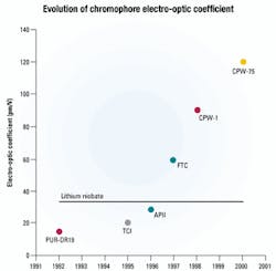
Satisfying a few of the above properties is not difficult. However, it is extremely challenging to satisfy all the criteria simultaneously. These properties are interrelated, and modification of one property often causes attenuation in the others. However, after careful design and synthesis, the CPW (Note: CPW, FTC, and PUR-DR19 are specific types of chromophores) chromophore family meets most of these criteria.Electro-optic polymers have experienced rapid growth in EO coefficient during the past decade. In Figure 1, the EO coefficient of polymers incorporating different chromophores is plotted as a function of time, with measurements performed at 1.06 microns. After 1997 and beginning with the FTC chromophore, these material systems have exhibited non-linear optical strength exceeding that of lithium niobate. Consequently, over the past decade there has been a sharp decrease in polymer modulator half-wave voltage (Vπ). The observed EO coefficient growth was the result of detailed investigations of chromophore-chromophore interactions in the polymer and experimental exploration of organic molecules exhibiting large second-order non-linearities.
In conjunction with increased non-linear optical performance, work on polymers has brought about significant reduction in material losses. Ridge optical waveguides fabricated from the polycarbonate CPW material system exhibited optical loss levels of 1.7 dB/cm at 1.55 microns.
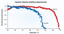
Moreover, recent explorations of cross-linked polymers incorporating the CPW chromophore demonstrate the ability to significantly enhance the material's thermal stability (see Figure 2). This figure shows dynamic material with temperature ramped at ~10°C/ minute and measurements of the second harmonic generation from a polymer film as a function of film temperature. These measurements reveal the variation of the polymer EO coefficient with temperature and, therefore, serve as a predictive tool regarding the modulator thermal stability.
These dynamic measurements were performed on polycarbonate (PC)/CPW films and on films incorporating crosslinked CPW chromophores (CPW -X1). As expected, the crosslinked material exhibited much greater thermal stability. In this case, the dynamic thermal stability was increased by approximately 40°C. The reduction in polymer electro-optic activity, as film temperature increases, arises from thermal de-poling of the material and not from chemical or mechanical changes in the film. Present estimates place the long-term thermal stability of the cross-linked material at 80 to 85°C with minimal impact on material non-linear optical properties.
The polymer modulator fabrication technology is mostly compatible with that of semiconductors. Three polymer layers make up the modulator: an ultraviolet (UV)-curable epoxy (the lower cladding), PC/CLD (active layer and core of the optical waveguide), and a low dosage UV-curable epoxy (upper cladding).
Figure 3a shows a schematic cross-section through the Mach-Zehnder arms, while figure 3b shows a photograph of one of the many chips already fabricated. For this present generation of demonstration devices, the polymer modulators are fabricated from the PC/CPW material system.
The three polymer layers are spun on a gold-coated, high-resistivity silicon substrate. Photolithography and reactive ion etching are used to define the ridge of the optical waveguides and the Y-junctions of the Mach-Zehnder. Utilizing an in-house poling procedure, the two arms of the Mach-Zehnder are poled anti-parallel to each other in order to facilitate the fabrication of a push-pull modulator. Lastly, electron beam evaporation and Au platting are used to fabricate the microwave structures that drive the traveling wave modulator.The modulator incorporates a single microwave drive while retaining push-pull operation. The radio-frequency (RF) source drives a single microstrip line feeding section that is split in two at the start of the interaction length by a broadband tee. In this fashion, the same microwave field drives both Mach-Zehnder arms and the push-pull operation is achieved by the anti-parallel orientation of the molecular dipoles. The lines, which are part of the 1-cm interaction length, typically exhibit an RF electrical loss of 0.7 dB/(cm-GHz5).
This loss is mostly due to frequency-dependent ohmic losses of the RF line. These losses also limit the bandwidth of the modulator to 40 GHz. At the end of the interaction length, the split lines are recombined by another broadband tee and the line is subsequently terminated on the chip. In order to eliminate connection parasitics, the modulator RF transmission line incorporates coplanar waveguide to microstrip transitions. The modulator input is connected via a K-connector.
A picture of a packaged device is shown in Figure 4. For this early prototype package, a K-connector was also used to provide DC bias to the modulator. The device is packaged with a polarization-maintaining fiber at the input and a singlemode fiber at the output.
Measurements of the modulator RF port DC Vπ revealed a value of 5.6 V at 1.55 µm. At this wavelength, the modulator DC extinction ratio exceeded 20 dB. The modulator frequency response was measured in the 2- to 50-GHz band using a network analyzer and a 50-GHz photodiode. The modulator 3-dB bandwidth was 34 GHz and response at 40 GHz was down 3.8 dB with respect to that at 2 GHz. The reduced frequency response is likely the result of additional losses incurred in packaging and line losses greater than typical.
Packaged modulator photo-stability was measured with an input optical power of ~20 mW on an earlier chip design. The modulator was illuminated for a period of one month. During this interval, the Vπ increased less than 10%. Moreover, due to the push-pull operation of the device, the anticipated modulator chirp is zero.
Present polymer modulator prototypes are competitive with other technologies in terms of frequency response and Vπ, and they demonstrate the potential of polymers for the 40-Gbit/sec modulation market. The next generation of polymer modulators will demonstrate its superiority to other competing technologies.
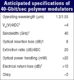
Based on prototyping work, ongoing polymer development, and modulator design and development, the market will soon have available a modulator with the characteristics outlined in the Table on this page, likely within the first quarter of 2002.
Dr. Hernan Erlig is principal scientist of electro-optics and Dr. Harold Fetterman is chairman and chief technical officer at Pacific Wave Communications (Los Angeles). They can be reached via the company's Website, www.pacificwaveind.com.


