Road to 40-Gbit/sec lightwave systems
A sensible evolutionary path calls for development of a roster of capable discrete devices.
JOHN KULICK, Agere Systems
The spectacular advances in lightwave communications have been so steady, so predictable, and so readily applicable that the industry often appears to take new technology for granted. Phrases such as "advancing at a rate exceeding a factor of 100 every 10 years" and "the cost of transporting a bit is decreasing by half every nine months" sometimes make it seem as though moving to the next-generation optical system is simple arithmetic: Multiply the earlier generation by a factor of two-or four.
Indeed, the industry has done such a good job of making it look easy that users have come to regard reliability, affordability, and capacity as entitlements. In response, the state of the art in less than two decades has soared from the 45-Mbit/sec systems of the early 1980s to today's 2.5- and 10-Gbit/sec systems. Now, 40-Gbit/sec systems are on the horizon. Some systems designers have already moved 40-Gbit/sec systems into trials. Last November, Lucent Technologies and Global Crossing Ltd. conducted a trial of a 40-Gbit/sec system across a 71-km fiber link connecting Brussels and Antwerp, Belgium.But scientists and engineers know that commercializing the next generation of optical networking is anything but simple. There are no "forklift upgrades" in engineers' toolkits, no way to multiply any critical system parameter without successfully addressing the many technical and economic challenges and tradeoffs inherent in the progress that people expect from lightwave communications systems.
Creating commercial 40-Gbit/sec lightwave systems with the same economy, reliability, and ease of use that people took for granted in earlier systems is a major challenge for the industry. It's going to be a lot harder to get to 40 Gbits/sec than it was to go to 2.5 and 10 Gbits/sec. As with any leap forward, the higher the speed desired, the more strenuous the demands on the technologies needed to realize the gain. And with the world clamoring for even higher speeds with quicker delivery of working systems, development intervals will be compressed, requiring creation in parallel of some components and system elements.The first step on the road to 40-Gbit/sec systems is to recognize some fundamental challenges and tradeoffs, among them:
- No direct-modulated sources are yet commercially available for 40-Gbit/sec operation, requiring externally modulated sources for now and in the foreseeable future. Significant advances in drive electronics may be required to achieve modules with internal modulation at 40 Gbits/sec. There aren't many integrated circuits (ICs) available today that have the voltage output needed to drive an external modulator at 40-Gbit/sec rates. The industry needs to move aggressively to create capable drive electronics.
- Designers of 10-Gbit/sec systems were really pushing the envelope to get reliable operation of fiber due to dispersion problems. Media impairment at 40-Gbit/sec rates is an even more significant challenge. The allowable dispersion penalty scales as the square of the bit rate. Thus, dispersion is 16 times more significant at 40 Gbits/sec than at 10 Gbits/sec. Polarization-mode dispersion (PMD) in particular could result in significant pulse distortion over distance. The fiber PMD characteristic should be below 0.5 psec/√km for fiber carrying 40-Gbit/sec traffic. Yet, much of the fiber in the ground typically exhibits 1-10 psec/√km . Many service providers cannot identify all of their fiber with certainty, much less characterize its properties accurately. Therefore, some systems may have to incorporate dispersion compensation to realize 40-Gbit/sec rates.
- Data coding techniques that operate with robustness at 10 Gbits/sec may be difficult to implement reliably at 40 Gbits/sec. Thus, it may require significant work to achieve reliable results.
- Greater integration of system components, especially into monolithic structures, while desirable, may be necessary to reduce parasitics and assure the speed and footprint requirements necessary for practical operation at 40 Gbits/sec. This effort may require breakthrough work in III-V materials.
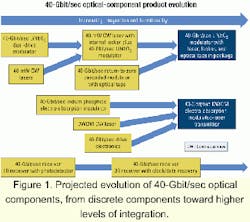
How does the industry face and overcome these challenges to deliver the 40-Gbit/sec systems customers are demanding? A rapid evolution of discrete components, starting with the strong base of existing 2.5- and 10-Gbit/sec system elements and using technological enhancements to drive toward a phased introduction of integrated circuitry (see Figure 1).
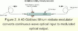
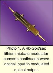
It makes sense to start with receivers and transmitters that are externally modulated, with ongoing research and development efforts to provide integrated modulation down the road. Fortunately, the industry has a strong foundation of excellent lithium niobate (LiNbO3) materials and technology, used extensively in today's 2.5- and 10-Gbit/sec systems. The characteristics of these devices are well understood, and the technology is robust and proven. The anticipated evolutionary path is to modify and optimize LiNbO3 modulators for 40-Gbit/sec operation.These 40-Gbit/sec LiNbO3 modulators, which support wavelengths from 1,525 to 1,565 nm, use an integrated Mach-Zehnder configuration to convert from continuous-wave optical input to modulated optical output, which reduces power requirements and eases the load on the laser transmitter (see Photo 1 and Figure 2). The second-generation modulator has lower voltage requirements, making 40-Gbit/sec operation somewhat less demanding on the material and driver circuitry.
In receiver technology, a fact of life is the higher the bit rate, the greater the loss of sensitivity. Add the sensitivity problem to the media impairments encountered at high bit rates, and achieving 40 Gbits/sec becomes an even greater design challenge. A typical solution to the photodetector problem is to increase bandwidth by using thinner material layers. But less absorbing material results in lower responsivity-as low as 0.2 A/W versus 0.8 or 0.9 A/W for a good detector. Clearly, a receiver needs an infusion of new technology to operate satisfactorily at 40 Gbits/sec.Polarization-dependent loss (PDL) is another major tradeoff in scaling up a detector to operate in a 40-Gbit/sec lightwave system. PDLs as high as 1.5 dB can be easily encountered from non-optimized detectors. By design, the waveguide structure yields a low PDL figure of less than 0.5 dB, highly suitable for 40-Gbit/sec operation.
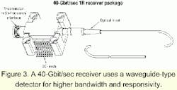
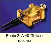
Reducing parasitics in the receiver circuit to improve performance is a top priority. Clearly, the solution is to keep interconnections and bonds short and close. Ultimately, the shortest paths can be achieved through integration of devices in monolithic structures. A waveguide-type detector lends itself far more handily to a future monolithic chip design than a surface-illuminated device.The initial component using this design results in a hybrid 40-Gbit/sec receiver, containing the detector and its associated wideband IC on a common platform (see Photo 2). The package design carries forward the waveguide philosophy in a pigtailed metal package with a single-ended V-connector (see Figure 3).
An optical amplifier also could eventually be integrated onto the same semiconductor substrate as the detector to boost the incoming signal and improve performance. For example, a second-generation integrated receiver circuit may include post-amplifier, clock and data recovery functions. Even further down the road, the use of indium phosphide (InP)-based III-V materials, among others, for the electronics portion of the receiver IC can lead to greater speed due to their high electronic mobility. Having a common material technology such as InP for both the electrical and optical functions could greatly increase the possibility of monolithic integration.
Successful design of 40-Gbit/sec transmitter devices will require several developments to occur in parallel. It starts with 40-mW continuous-wave lasers, which are available now. Even as these devices can satisfy current market needs, industry development is moving ahead rapidly on first-level integrated devices combining the 40-mW laser with an internal wavelength locker and a 40-Gbit/sec LiNbO3 modulator.
Development efforts are aimed at providing the marketplace with improved devices using greater levels of integration, for example, the combination of a 100-mW distributed-feedback laser transmitter in an integrated 40-Gbit/sec transmitter package that also includes the LiNbO3 modulator, a wavelength locker for increased stability, and optical taps for monitoring power and providing controls for design features.
These types of devices will appear by the end of 2002.
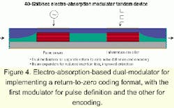
The marketplace guides these and other developments in 40-Gbit/sec systems. Designers who want the ultimate overall performance for their systems-particularly in long-haul systems where dispersion is a major factor-will use LiNbO3 modulators that have superior extinction ratios compared with electro-absorption (EA) modulators. What's more, many designers are looking to a return-to-zero (RZ) coding format as the choice for 40-Gbit/sec systems, because it offers a more robust method to identify and recover the signal. Non-return-to-zero is the preferred format for today's lower-bit-rate systems.One approach to realize that is to use two discrete modulators in tandem, with the first one to carve out a train of pulses and the second one to code them in the desired RZ format (see Figure 4). Initially, this approach will be realized using LiNbO3 modulators, because this technology is more mature. RZ-capable modulators will be an important element in 40-Gbit/sec systems. Eventually, the modulators themselves could be built with EA technology, based on InP materials (see Figure 5). The InP-based modulators require lower drive voltages than LiNbO3-based modulators and at the same time facilitate integrating the modulator on the same substrate as the laser-for a true monolithic source. This combination can make it possible to entertain electro-absorption-modulated-laser (EML) transmitters at 40 Gbits/sec, in the same manner that is currently being demonstrated at 10 Gbits/sec today. This development may also make it possible to achieve performance levels now associated only with LiNbO3 materials and techniques and at potentially lower cost.
Long haul is not the only application on the horizon for 40-Gbit/sec systems. With anticipated continued high growth of Internet traffic, there is an emerging trend to connect routers at very short distances-in single-digit kilometers-with the highest-speed lightwave systems available. This need could spur further development and short-haul application of 40-Gbit/sec components based on EA technology.
What's more, these EA-based devices may have a smaller footprint, and simpler drive electronics, than comparable LiNbO3 devices-crucial considerations for designers of high-capacity connectivity solutions that need to share space with other equipment in crowded offices. This emerging application will continue to develop its own requirements, potentially as demanding as those required for long-haul applications. These components can help to provide solutions for these demands, as well.
In the Information Age, information is the life-blood of the global economy, and networks are its veins and arteries. Just as lives literally depend on the telephone, the health and vitality of the economy requires capable networks that meet the most exacting demands for cost, capacity, and reliability.
John Kulick is a senior marketing manager in the Optoelectronics Group at Agere Systems (formerly the Microelectronics Group of Lucent Technologies) in Breinigsville, PA.

