Modulation advances drive next-generation DWDM systems
Indium phosphide enables promising devices for modulation and optical TDM implementations.
Hava Volterra and Uzi Koren
CyOptics Inc.
Manufacturers face several technical challenges in the race to develop the next generation of DWDM transmission technology for 40-Gbit/sec and ultra-long-haul (ULH) systems. Signal degradation due to chromatic and polarization-mode dispersion, noise, and fiber nonlinear effects as well as the limitations of existing electronics devices are all major problems that require solutions.
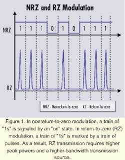
New components are enabling optical-data modulation and multiplexing techniques that could help backbone traffic travel longer distances at higher speeds. These emerging data-modulation schemes hold promise for continued progress in optical networking.Most optical data-transmission systems in operation today use a non-return-to-zero (NRZ) data-modulation scheme (see Figure 1). For transmission rates up to 2.5 Gbits/sec and first attempts at 10-Gbit/sec systems, NRZ modulation has been adequate, offering simple and cost-effective implementations and good signal integrity. But as equipment designers strive to increase channel counts and transmission speeds and distances, the associated technical challenges such as high-speed electronic signal generation, high-speed clock recovery, chromatic dispersion, polarization-mode dispersion, four-wave mixing, and self-phase modulation demand new solutions.
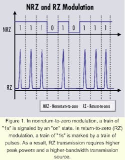
To address the challenges of higher-speed and longer-distance optical networking, many systems designers are selecting various forms of return-to-zero (RZ) modulation for their transmitters. In RZ modulation, a "1" is signaled by a pulse, while a "0" is signaled by lack of a pulse (see Figure 1). Characteristics of an RZ signal include its pulsewidth, peak power, and shape. The peak power of RZ transmission is typically higher than the peak power in NRZ transmission to provide an adequate total power per time slot. For narrower RZ pulses, higher peak powers need to be used.
RZ signals offer several advantages in optical transmission, which can result in higher signal-to-noise ratio and lower system bit-error rate, translating to higher overall system performance. With correct system design, RZ signals offer better immunity to fiber nonlinear effects. In addition, the effects of polarization-mode dispersion, which is dispersion due to the differences in diffraction index in different directions along the fiber, are significantly reduced when RZ modulation is used. The pulsed nature of the RZ signal can also reduce interaction effects between DWDM channels, such as cross-phase modulation, making it suitable for very-high-channel-count systems.
Equipment vendors and researchers have announced successful results from experiments involving variants of RZ modulation. One variant is soliton pulses-waveforms with special characteristics that propagate over very long distances. Tedons are another area of research. These are short pulses that undergo negative dispersion before transmission.
Solitons have been the focus of much research. Solitons are RZ pulses matched to the transmission fiber, so that the effects of self-phase modulation (a nonlinear effect in which the instantaneous power level of the pulse affects the fiber diffraction index and consequently the speed of signal propagation) and other nonlinear effects cancel out the effects of chromatic dispersion, resulting in a pulse that can propagate almost indefinitely through the fiber. In the early 1990s, it was shown that these waveforms could propagate over tens of thousands of kilometers of fiber, but the requirement to use a uniform fiber to maintain the soliton shape meant that the application had been limited to trials in the more tightly controlled submarine fiber links. Today, adaptive dispersion-management techniques are used to allow the waveforms to propagate over the mixed fiber plant found in terrestrial networks, and because solitons are highly tolerant to fiber nonlinear effects, they are expected to emerge as one of the key enabling technologies for successful OC-768 (40-Gbit/sec) systems.Figure 2. For transmission, four short-pulse10-Gbit/sec return-to-zero (RZ) data streams are run through delay lines, then combined. The delay lines cause the four signals to interleave, creating one 40-Gbit/sec data stream. In receiving the data, polarization-insensitive, indium phosphide modulators serve as gates to demultiplex the data into four separate 10-Gbit/sec data streams before conversion into electronic signals. Thus, the same components used to implement RZ modulation can be used to implement optical time-division multiplexing.
Tedons are a more recent innovation. They are a form of pseudo-linear RZ transmission in which an RZ signal consisting of very short, high-peak power pulses undergoes strong negative dispersion before transmission, thereby reducing peak power and creating a signal that looks like white noise. This dispersed signal is largely immune to nonlinear effects, because of its low and fairly even power levels. As the signal travels through the fiber, positive chromatic dispersion acts to recreate the original signal. Thus, the signal at the receiver is a faithful reproduction of the original signal. This method has yielded excellent results in experimental transmission of 40-Gbit/sec signals over long spans of conventional optical-fiber plant.
These experimental results argue for use of various flavors of RZ modulation for high-performance transmission. In fact, many of the new systems being developed today for 40-Gbit/sec and ULH transmission, use some form of RZ transmission as their modulation format. It seems clear that RZ modulation will play an important role in future DWDM systems, and that in turn creates the need for new generations of optical components.
An additional method of transmitting data at very high speeds is optical time-division multiplexing (OTDM). Although OTDM has been studied in laboratories for more than 10 years, only with the transition to 40-Gbit/sec transmission have its advantages become commercially compelling.OTDM takes advantage of the fact that the bandwidth of optical components is increasing faster than the bandwidth of electronic components. It allows the system designer to overcome the speed limitations of a system's electronic components by creating several lower-speed electronic data streams and multiplexing them together in the optical domain.
While it is possible today to obtain commercial 10-Gbit/sec electronic drivers, 40-Gbit/sec devices are not yet available. Using OTDM, several 10-Gbit/sec data streams can be multiplexed to form a 40-Gbit/sec optical data stream, which is then transmitted through the fiber. The signal is then optically demultiplexed into separate 10-Gbit/sec data streams before conversion to the electronic domain (see Figure 2).
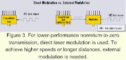
To understand the basic structure of RZ transmitters, it is helpful to revisit the architecture of NRZ transmitters, which typically use one of two forms of modulation: direct modulation or external modulation. Direct modulation is used for lower-performance systems, while external modulation is used for higher-performance systems (see Figure 3).
In direct modulation, the transmission lasers are turned on and off to create an NRZ data stream. The advantage of this method is its simplicity; the disadvantage is that this method introduces changes in the frequency of the transmitted light or "chirp." Chirp causes higher chromatic dispersion and therefore limits the distance a signal can travel. For OC-12 (622-Mbit/sec) and OC-48 (2.5-Mbit/sec) systems, direct modulation may be sufficient; but for higher speeds or longer distances, external modulation is generally needed.
For the highest-performance systems, external modulation is used. In externally modulated transmission, the laser is kept constantly on or in continuous-wave (CW) mode, while an external modulator acts as an electronic shutter to turn the signal on and off. Integrated devices also known as electro-absorption modulated lasers (EMLs) are sometimes used as alternatives to true external modulation, but performance is limited. In contrast, a true external modulator can be optimized for high performance, and it doesn't suffer from the compromises required when an integrated device is constructed.Most conventional, externally modulated systems use modulators made of lithium niobate (LiNbO3). New indium phosphide (InP)-based modulators, however, offer the same high performance but have a much smaller size and significantly lower driver voltage requirements (see sidebar, "What is indium phosphide?"). These InP-based modulators will also lead to hybrid devices that integrate a laser and modulator into a compact, lower-cost device.
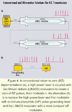
In high-speed RZ transmitters, two functions-pulse generation and data modulation-are handled separately (see Figure 4). Conventional RZ transmitter implementations utilize a high-power laser, coupled with two LiNbO3 modulators. One modulator creates a train of RZ pulses, and the other one performs data modulation. The drawbacks of this implementation are the size, cost, and need to work with a very-high-power laser to achieve the high peak power required in RZ transmission.
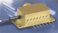
An alternative is an InP pulse-generating laser (PGL) to create the pulse train. The PGL is a more compact device and can generate higher peak powers and shorter pulsewidths than the laser/LiNbO3 combination (see Photo). The PGL is then coupled with a data modulator (either InP or LiNbO3) to create the modulated RZ signal.Conventional RZ transmitters use a high-power laser, coupled with two lithium niobate (LiNbO3) modulators. An alternative is to employ an indium phosphide (InP)-based, pulse-generating laser like the one shown here and a LiNbO3 or InP-based data modulator.
For OTDM implementations, component size and power requirements are particularly important because of the large number of components required. InP components are uniquely suitable in this respect. In addition, the OTDM demultiplexer needs to be polarization-insensitive, because the polarization of a signal that has traversed many kilometers of fiber is time-varying and unpredictable. For this reason, LiNbO3 modulators, which are sensitive to light polarization, are not suitable for OTDM de multiplexing. In contrast, InP modulators are polarization-in sensitive, making InP modulators a good component choice for OTDM implementation.
The move to higher optical-transmission speeds and longer transmission distances requires new methods of data modulation.
Transmitters that utilize RZ modulation and OTDM are likely to be deployed in many leading-edge systems. New components, based on InP technology, will play a key role in this deployment.
Hava Volterra is vice president of marketing and business development at CyOptics Inc. (Burlington, MA). She can be reached at [email protected]. Uzi Koren is chief technology officer at CyOptics. His email address is [email protected].
Indium phosphide (InP) is a member of the III-V family of semiconductors. III-V materials are binary crystals with one element from the metallic group 3 of the periodic table and one from the nonmetallic group 5. The family includes gallium arsenide (GaAs), InP, gallium nitride (GaN), indium antimonide (InSb), and indium arsenide (InAs). Some of these binary compounds are known for their high mobility of electrons and holes, which in the case of the best known example-GaAs-facilitates the operation of very-high-speed electronics.
A focus of development since the early 1980s, InP today is used as a platform for a wide variety of fiber communications components such as lasers, light-emitting diodes (LEDs), semiconductor optical amplifiers, modulators, and photodetectors.
III-V compounds have a cubic lattice-like structure with atoms in each corner. InP, for example, features alternate indium and phosphorous atoms. As a semiconductor, InP has an energy bandgap, which makes it opaque for light-energy levels higher than the bandgap and transparent for light-energy levels below the bandgap. The bandgap of many III-V materials, including InP, is also known as a "direct" bandgap. This means the quantum transitions that take place when a photon is absorbed or emitted do not require any quantum change in the momentum of carriers; these transitions occur much more readily, making the material highly suitable for fabricating devices such as lasers or LEDs. This direct bandgap supports optical gain as required for lasers and very high absorption-photons can be absorbed within very short distances-making functions such as data modulators or fast photodetectors easy to implement.
A family of materials, including indium gallium arsenide (InGaAs) and indium gallium arsenide phosphide (InGaAsP), share the same 5.87Å (angstrom plus a common unit of measurement or molecules-1 angstrom = 10-10 meter) lattice constant as InP, allowing epitaxial processing on top of the basic InP wafer. These materials may be used to provide attributes such as electrical confinement to improve laser efficiency and optical confinement to provide active (gain or absorption) and passive (transparent) optical waveguide functions. Other nonmatched materials may also be grown in thin layers to add useful properties such as quantum effects and strain. In the case of InP, these materials allow the fabrication of high-efficiency quantum-well lasers.
One of the key advantages of InP is device size. Because the refractive indices of InP and its ternary (InGaAs) and quaternary (InGaAsP) derivatives are relatively higher than for other optical materials, bends can be made much sharper and smaller.
As the energy bandgap is also closer to light-energy, electro-optical effects are stronger than in other materials (which again translates into shorter distances and lower drive voltages). A downside of these smaller geometries is that it becomes more difficult and lossy to couple to optical fiber. That is overcome by means of taper structures at the interfaces to match the optical mode size at the InP chip facets with the fiber ends.
The result is extremely small devices; die sizes are typically less than 5 mm. For the simple types of functions discussed here (i.e., lasers and modulators), die sizes are considerably less than that at 1 mm or smaller. InP processing complexity compares favorably to that of commodity silicon chips, with less than 16 stages of photolithography.
As a semiconductor, InP has strong potential for creating integrated devices. That includes combining different active optical elements together-such as lasers/modulators/amplifiers and optical switches/interferometers-along with passive waveguides. Moreover, current development work on heterojunction bipolar transistors holds strong promise for combining optical elements with electrical drive circuitry. This integration could provide powerful, cost-effective solutions for implementing high-speed DWDM and optical time-division multiplexing systems.
