VCSELs demonstrate path to dense optical interconnects
Using a hybrid VCSEL/ASIC package, a 36-m optical bus aggregates bandwidth over 32 synchronous channels, providing built-in redundancy and 10-15 bit-error rate.
WILLIAM D. LINDSAY, TeraConnect
Interconnects are the data highways between collocated blocks of computer equipment. As the individual blocks grow larger, both in size and processing power, more traffic needs to flow between them at ever-faster rates. Otherwise, data starts to back up like rush hour traffic.
In the era of surging Internet demand, denser storage-area networks (SANs), and higher-speed server farms, the individual processing units in these systems have become very large indeed. IP router and optical switch designers, for example, envision devices with more than a thousand ports-each capable of 1 Gbit/sec or more. To communicate with one another inside a switching center, those devices will require an interconnect with vastly higher bandwidth capacity than those available today-in the tens and even hundreds of gigabits per second. The same is true for SANs and server farms. In all these cases, the individual boxes must somehow pass data back and forth among themselves at a speed higher than the rate at which they send data to the outside world.As equipment designers have sought solutions to this bottleneck, some lessons have become clear. First, interconnects between collocated blocks of equipment will not be single-channel links. A 10-Gbit/sec cable can only deliver 10 Gbits/sec. Yes, higher-speed signals can be demultiplexed over multiple single 10-Gbit/sec links, but that merely multiplies the cost of the links, the unit cost of which is high. Multiple lower-speed links are also difficult and expensive to interface, requiring the use of complex optoelectronic circuitry for demultiplexing and multiplexing.
A second lesson is that these high-speed interconnects will be made out of glass rather than copper. Copper attenuates signals at shorter distances as signal frequencies increase (within 6 m in the 1-Gbit/sec range). Yet, switching centers, server farms, and SANs need to move data at higher frequencies because they are physically larger and have more data to move.
All of which helps explain why equipment makers have increasingly turned to vertical-cavity surface-emitting lasers (VCSELs) as perhaps the ultimate bandwidth bottleneck breaker. A recent demonstration highlighted how VCSELs make excellent components in transceivers built as massively parallel, and very small, optical connections.
The smaller size promised by VCSEL-based devices means more fibers per cable, which means more bits can be pumped through at any given clock rate. Turn up the clock from 2.5 Gbits/sec to 10 Gbits/sec on a cable driven by a single laser and cable throughput is only increased four-fold. Turn up the clock rate by the same amount on a cable with 32 channels and throughput is multiplied 128 times. No wonder the market for VCSEL-based transceivers has exploded, from $262 million in 1999 to a projected $14.1 billion in 2009, according to market researcher ElectroniCast Corp. (San Mateo, CA).As their name implies, VCSELs are vertical cavities, 850 microns deep, etched into the surface of a planer gallium arsenide substrate. The size of the cavity is important because lasers work by the mutual reinforcement of lightwaves as they reflect back and forth inside a container of dimensions equal to an integral number of quarter wavelengths. In this case, the inside surface of the cavity is built up with layers of semiconductor materials, having alternatively high and low indices of refraction.
In the demonstration example, each of 36 layers was a quarter-wavelength thick, producing a cavity surface of nearly perfect reflectivity. When current is applied to this surface, the resulting light reflects back and forth within the cavity, causing the light to self-amplify via constructive interference. The mirror at the top of the cavity is slightly less reflective than the mirror at the bottom-once the energy buildup reaches a threshold, the light penetrates the top mirror in a beam that is perpendicular to the plane of the substrate.
Beam divergence is only 11 degrees and the numerical aperture of the angular exit is well matched to the cross-sectional geometry of the fiber. That means the beam can travel across a gap of up to 500 microns and still shine more than 80% of its light into the fiber cable, which can carry the signal up to a mile, depending on the frequency of the light. That compares to 10% for traditional edge-emitting lasers, which require the help of coupling optics to refract and reflect the light back toward the end of the fiber.Another reason for using VCSELs is that they can be modulated directly from input current. Conversely, edge-emitting lasers require external optical modulators that respond more slowly to changes in signaling current and add size and expense.
Cost savings are in fact the most compelling advantage of using VCSELs. A single 3.5-inch substrate yields more than 20,000 lasers for about $80,000-roughly the price of eight edge-emitting lasers. Even so, the most expensive part of building an optical transceiver, and the source of greatest cost savings, is not in the fabrication of the lasers, but in their packaging and optical alignment. That's because by using standard optoelectronic fabrication techniques, manufacturers can simultaneously slice and integrate several thousand lasers with their electronics and mechanical packaging. That's much less expensive than dicing each device separately, packaging it, and performing the delicate task of aligning every single laser with its own output fiber.
In the demonstration mentioned here, a 125-micron pitch (pixel separation) was achieved by photolithographic etching of a 16x20 VCSEL array on the transmit side and a 16x20 pin diode array on the receive side of a substrate. It was therefore possible to precisely align all 640 elements as a unit against 640 fibers. Contrast that with the alternative: individual alignment of 640 separate elements twice (once on each end of the interconnect)-a prohibitively expensive solution for wide-scale commercial deployment.
The goal of the demonstration was to show the feasibility of VCSEL-based massively parallel optical interconnects and at the same time illustrate their inherently superior reliability, scalability, and lower cost-of-manufacture and deployment. The demonstration platform was essentially a working model, using (or adapted from) off-the-shelf parts, that could be readily adapted to a commercial product that could be manufactured using a routine production process.The technology demonstration replaced a 6-m copper cable connecting two servers with a 36-m fiber-optic bus. The bus consisted of 640 individual multimode fibers allocated as four banks of 40 channels. The additional banks provide for fail-safe operation or can be used in combination with the others in an add/drop multiplexer configuration.
Data moves across the bus as 40 synchronous bits-four 8-bit bytes, plus an additional byte for framing and error correction. At a clock speed of only 200 MHz, the interconnect provides 6.4 Gbits/sec of aggregated bandwidth. (Initial production models would most likely implement clock rates of 1.25 and 2.5 Gbits/sec with correspondingly higher aggregate throughputs.)
Each bit is transmitted over two fibers, using differential optical signaling, a technique for reducing bit-error rates (BERs). In this technique, a bit registers as the difference in amplitude between two signals transmitted 180 degrees out of phase with each other. Since both members of each pair are affected in common by noise and signal drift due to temperature, they respond in tandem to those effects. That means that amplitude differences remain constant, except when varied by the digital encoding, even in the presence of drift and noise. In the demonstration, BERs were 10-15, three orders of magnitude less than without differential optical encoding.
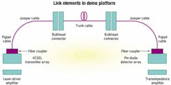
The overall layout of the demonstration model was straightforward, as shown in Figure 1. Each end of a 640-fiber ordered fiber array (OFA) is aligned to a VCSEL-based transceiver via a series of cables and connectors, including an alignment fixture and fiber coupler, as described in more detail below. Completion of the circuit between the active devices and the alignment fixture included a customized bulkhead connector as well as off-the-shelf jumper cables, backplane connectors, and pigtail connectors. (To simplify the diagram only one side of the transceiver is represented on each end of the interconnect.)
Even using an OFA, alignment of the transceiver emitters and detectors to their respective fibers remained a key challenge, as did the design of the transceiver itself.
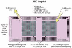
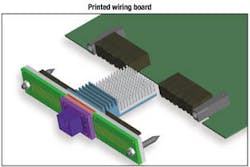
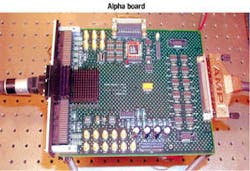
The transceiver is implemented as a hybrid package consisting of two layers bonded together: (1) an optical layer containing two adjacent arrays, the 16x20 VCSEL emitter array, and the 16x20 pin diode detector array and (2) an application-specific integrated circuit (ASIC) layer underneath containing 100,000 transistors. Figure 2 shows the footprint of the ASIC. The 12,058x5,384-micron package is bonded to a 6x1-inch printed wiring board (PWB) providing fanout of the 196 signals and guide pins that attach the PWB to the rest of the server interface board (see Figure 3).The main reason for the large size of the IC package and PWB is to provide room for connector fanout. With only 100,000 transistors, the ASIC is relatively empty, leaving ample room for future value-added functions such as data encryption and quality of service. Existing functions include two amplifiers: a transimpedance amplifier for converting currents received from the diodes into standard low-voltage differntial signaling (LVDS) signal levels, and a laser-driver amplifier that essentially does the reverse: converts LVDS signals into currents that can drive the VCSELs. Selection of feedback resistance in the transimpedance amplifier determines bandwidth from 0.4 to 6 GHz, while the laser-driver amplifier allows operation of the VCSELs up to 1 GHz. Additional on-chip functionality includes:
- Integrated 8-bit/10-bit encoding.
- Differential optical signaling.
- Bank switching between four banks of 32 channels each.
- Variable-gain (laser brightness) and modulation control of the VCSELs.
Insofar as a demonstration platform required bonding two ICs together, both of which generate heat, temperature was an initial concern. Various countermeasures, such as the placement of heat-sinks and heat-spreaders, and performing extensive thermal simulation counteracted these concerns. The mechanical properties of the optical layer itself, which was very thin and compliant on its backside, provided certain benefits. There were no problems in transferring heat from this layer through the ASIC to an off-the-shelf heat-sink without active cooling.
As mentioned previously, one of the advantages of using arrays (whether as fibers, emitters, or detectors) is that it is faster, easier, and less expensive to align elements as units rather than individually-a point the demonstration aimed to prove. The major goal of the demonstration, therefore, was to implement an easily repeatable method of simultaneously shining 320 10-micron-wide VCSEL lasers onto the ends of 320 50-micron-diameter fibers at one end of the interconnect. The reverse-shining the lights from each of those fibers onto each of their respective detectors-had to be accomplished at the other end of the interconnect.
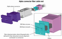
Figure 4 illustrates how this goal was accomplished via the modification of a MT ferrule-type connector shell. A plate was affixed to the shell into which were made 640 holes, each of which was photolithographically aligned with its appropriate transceiver element (either a VCSEL or a detector). Aligning the fibers required threading them through the holes-manually here-but that could easily be converted into an automated process. Figure 5 is a photograph of the complete transceiver assembly installed as a board edge connector with its interface cable attached.
Over the eight-week period of the demonstration, the model interconnect, employing 640 massively parallel optical devices, operated with no bit errors detected. The demonstration proves a number of things-not the least of which is the broad variety of skill sets that play a role in building these devices. That includes everything from precision machine design to solid-state physics. It also proves that the economies of scale inherent in semiconductor fabrication can apply directly to high-speed data interconnects.
From now on, interconnect speed and functional robustness will grow geometrically relative to cost, just as they do in computing. Rather than prove the persistent bottleneck, interconnect performance will now grow in step with the systems they serve.
William D. Lindsay is director of product marketing at TeraConnect (Nashua, NH). He can be reached at [email protected].
Whatever the purpose, all articles, product announcements, and advertisements in Lightwave can be reprinted to suit your informational needs.
For information, contact
Kathleen McIntosh at: (603) 891-9203, fax (603) 891-0587, or e-mail: [email protected].

