Evolutionary trends in pluggable optical modules

Enabled by advances in uncooled DFB laser technology, serializer/deserializer (SerDes) ICs, and transmitter/receiver optical subassembly (TOSA/ROSA) packaging, pluggable optical modules are now firmly established in the design of optical interfaces for LAN, access, metro, and core networking equipment. A variety of multisource agreements (MSAs) have defined pluggable optical modules that provide transmission rates of 155 Mbits/sec to 10 Gbits/sec over distances ranging from very-short-reach (VSR) 600 m to long-reach (LR) 80 km. The MSAs have provided standardization of optical modules and components and assured second-sourcing availability and compatibility. Additionally, they have enabled new features such as active pluggability, increased port density, reduced power consumption, faster design-in time, and overall reduced cost.
To take further advantage of pluggability, system OEMs and optical-module developers are pursuing new module designs that not only extend the application range—for example, very-long-reach (120 km)—but provide further integration of optical interface functionality such as forward error correction (FEC) processing and Layer 1 framing. Pluggable optical modules with integrated link processing can significantly reduce port costs for system OEMs and simultaneously enhance line-card port modularity and configuration flexibility.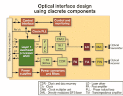
In the beginning, optical interfaces were designed and developed by system OEMs using discrete components and custom IC devices. (A typical optical interface architecture using discrete components is illustrated in Figure 1.) Key components in the receive path include the PIN diode or avalanche photodiode (APD), transimpedance amplifier (TIA), post-amplifier, clock and data recovery (CDR) unit, and demultiplexer. In the transmit path, key components include the multiplexer, clock multiplier unit (CMU), laser driver (LD), and a laser source. An uncooled 1310-nm directly modulated DFB laser (DML) is typically used for short-reach (SR) applications. For longer-reach applications, the LD/DML is replaced with an external modulator and driver and a cooled 1550-nm continuous wave laser source.
Additional devices are included in the design for optical-signal control and monitoring (e.g., laser bias and temperature control) and for controlling digital performance (e.g., FIFOs and filters for jitter control). The optical interface design typically includes a Layer 1 framing and overhead byte processor device for SONET/SDH digital link fault management and performance monitoring. This device as well as optical-signal control and monitoring devices require a control interface to the system controller, typically through a local or I2C bus. Finally, components are included for power-supply conditioning.
Whenever a new feature or application was required by the end user, system OEMs needed to undertake a completely new design and development of the optical interface. Since that required significant engineering and manufacturing resources, there was clear motivation for system OEMs to simplify the optical front-end design.
The optical-module MSA approach fills this need. The typical MSA describes a common pin interface and form factor for the module in question. Several module MSAs have been established in the past several years. While they often compete for the same or similar applications, each has unique design value propositions.
In the evolution of the 10-Gbit/sec optical front-end, the most dominant MSA to date is the 300-pin optical transceiver with integrated SerDes—also known as an optical transponder. This MSA effectively defined a boundary around the optical front-end components and specified the network-side optical interface and equipment-side parallel electrical data and clock interface (see Figure 2).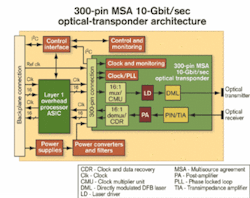
Several key improvements in the optical front-end design have resulted in the evolution from discrete components to the 300-pin MSA optical-transponder architecture. Device integration has occurred for lowering power consumption, shrinking footprint, and reducing overall cost. In the receive path, the demultiplexer and CDR have been integrated into a single device and the TIA is often integrated with the PIN/APD. In the transmit path, the multiplexer, CMU, and FIFO have been integrated into a single device. The most recent evolutionary step by IC suppliers has been to integrate the receiver and transmitter SerDes functions into a single-chip transceiver device. The transceiver device not only provides reduced power consumption and board real estate requirements, but it also enables new features such as on-chip data-signal loopbacks. Performance of the single-device transceiver, however, with respect to channel crosstalk and SONET/SDH jitter generation requirements, remains to be confirmed.
One of the key benefits of the 300-pin MSA is it provides a complete optical interface module with an easily managed interface. The electrical clock and data interface operate over 16 parallel channels at 622–669 MHz, which simplifies printed-circuit-board design. This electrical interface is compatible with the Optical Internetworking Forum (OIF) SFI-4 and IEEE XSBI specifications, which numerous IC suppliers have adopted. It supports SONET/SDH rates (with or without FEC) and the 10-Gigabit Ethernet (10-GbE) XSBI interface. The optical interface is compliant with ITU-T G.691 specifications. Suppliers currently offer 300-pin MSA transponders for applications ranging from VSR to LR2. The 300-pin MSA form factor ranges from 5×5×0.7 inch to the most recently introduced small form factor (SFF), 2.2×3×0.53 inch.
The 300-pin MSA 10-Gbit/sec optical transponder is well matched for the client-side VSR, SR, and intermediate- reach (IR) optical interfaces. It is increasingly being used for both client-side and network-side LR interfaces. For ultra-long-reach applications and optically amplified DWDM systems, discrete component-based interfaces continue to dominate the market due to system OEM proprietary design features for system performance and control. Work is under way to move the 300-pin MSA to the next stage: 40 Gbits/sec.
Yet, in the continuing effort to reduce the cost of the optical front-end, the 300-pin MSA optical transponder has been a target for simplification or complete elimination. The device's 16-channel SerDes is mainly included to enable low-speed board-level interconnection between the optical transceiver and Layer 1 framer IC. In high-volume applications, such as VSR and SR links, the SerDes device becomes a significant factor in terms of overall cost, power consumption, and board space. This consideration has led the evolution of MSA electrical interfaces in two distinct directions: a four-channel parallel interface and a single 10-Gbit/sec serial interface.
The 16-channel SerDes in the 300-pin MSA optical transponder can be viewed as two stages of four-channel SerDes devices. By eliminating one of the four-channel stages and operating the remaining stage at four times the 16-channel rate, the result is a four-channel parallel SerDer electrical interface architecture.
For 10-GbE applications, XENPAK and similar X2 and XPAK MSAs have been established based on the four-channel SerDes architecture. XENPAK migrates from the 16-channel parallel XSBI to the four-channel parallel XAUI. The XAUI interface was chosen for XENPAK because it has a low pin count, does not require a clock, and with a bit rate of 3.125 Gbits/sec, can be readily implemented in standard CMOS. Furthermore, the data across the XAUI is self-aligned, meaning that the SerDes device automatically deskews the four channels. That enables a reduced transponder form factor and simpler board-level implementation. In addition, XENPAK allows a higher port density over the 300-pin MSA, with up to eight ports on a typical line card.
For SONET/SDH applications, the OIF recently completed SFI-4 Phase 2 specifications, which define a four-channel parallel electrical interface supporting SONET/SDH standard rates with or without FEC. It is not clear if the Phase 2 interface will find application by system OEM and optical-module vendors that may opt for direct 10-Gbit/sec serial designs.
While the four-channel SerDes architecture was pursued to reduce transponder cost, power consumption, and size, a more radical approach is to eliminate the SerDes altogether. This was done in the SFF MSA for 2.5-Gbit/sec and lower rates and most recently in the XFP MSA for 10-Gbit/sec applications. The XFP MSA optical transceiver provides a serial 10-Gbit/sec electrical interface (called XFI), which places the SerDes external to the transceiver module on the line card either as a standalone device or functionally integrated in the framer IC. A main objective of the XFP MSA is to provide specifications for an active pluggable SFF 10-Gbit/sec optical transceiver that is protocol-agnostic (i.e., can serve 10-GbE, Fibre Channel, and SONET/ SDH applications).
The XFP module typically consists of TOSA/ROSAs and a single-chip transceiver IC. The transceiver IC provides the CDR function on the receive paths, plus a post-amplifier on the optical receive path side. It also provides the I2C bus interface for transceiver control and monitoring. The TOSA includes an uncooled laser diode and driver. The ROSA includes the PIN diode and TIA.
The key value proposition of the XFP design is a combination of three factors: size, flexibility, and cost. With the eliminated SerDes and reduced pin count, the resulting smaller form factor will permit up to 16 ports on a typical single line card. The eliminated SerDes and the TOSA/ROSA packaging lead to reduced bills of material and manufacturing costs. The protocol/rate-agnostic and active pluggable features enable the host line card to be designed for a mix of applications and provisioned in the field. An optical interface design using the XFP architecture is shown in Figure 3.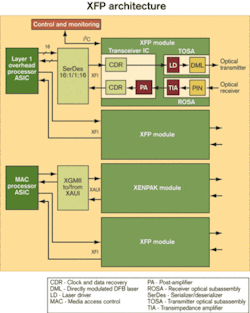
One disadvantage of the XFP design is it currently requires uncooled or quasi-cooled laser sources to meet power consumption requirements. Only VSR, SR, and IR applications can be supported currently. Whether LR2 and DWDM applications can be achieved within the XFP MSA standard form factor will depend on future laser-diode technology evolution. Additionally, using the XFP module requires the system OEM to design line cards with 10-Gbit/sec traces. Extra design effort is required to manage trace lengths and crosstalk noise on the line card, which can add design time and require additional ECAD tools and design expertise.
In the evolution to the next-generation optical module, two electrical interfaces will most likely prevail. For 10-GbE and Fibre Channel applications, optical transponders are migrating from the 16-channel parallel XSBI to the four-channel parallel XAUI using XENPAK. Some system OEMs may decide to evolve their line cards from XSBI directly to XFI using XFP modules. The selection process for which evolution path to pursue is complex, and consideration must be given to a variety of application and design requirements.
For SONET/SDH applications, the current 16-channel parallel SFI-4 electrical interface will most likely remain a dominant solution in either 300-pin MSA optical transponders or as an external device with X2 or XFP modules. System OEM makers are now seeking to enhance the 300-pin MSA optical transponder with such features as active plug-in. As shown in the Photo, this module contains all necessary board-level control and management to enable the 300-pin SFF MSA optical transponder to be actively inserted and provisioned in the deployed host system. One key benefit of the design is it allows system OEMs to provide active pluggable optics using today's mature 300-pin MSA transponders for VSR to LR2 applications well in advance of emerging XFP modules.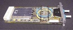
Future enhancements to optical-modules designs of this type include the incorporation of Layer 1/FEC processing ICs, which increase module functionality and fiber reach. The cost is a larger module size, increased chip count, and increased power consumption. Additional enhancements such as electronic dispersion compensation devices are also envisaged for inclusion in future-generation optical modules enabling 10-Gbit/sec very-long-reach applications.
In the evolution of optical-module design, two concurrent but distinct trends have emerged: more integration and less integration. Optical-module solutions based on a minimally integrated architecture such as XENPAK, XFP, and SFP are being adopted mainly in systems where increased port density, enhanced port configuration flexibility, and reduced port cost are key evolutionary forces, such as in enterprise LAN/SAN equipment. Highly integrated optical-module solutions such as the 300-pin MSA optical transponder have dominated and will continue to dominate in systems where application reach flexibility, performance, and cost are key drivers, such as in metro optical transport equipment.
System OEMs are now pursuing active pluggable integrated solutions that enable port configuration flexibility while simultaneously enhancing performance and application reach flexibility. For ultra-long-haul DWDM system applications, discrete solutions are still being used in the network optical front-end architecture due to the proprietary design of the system.
While the MSA approach has provided the benefits of standardization for the optical front-end, it can be clearly observed that no single solution fits all applications and system OEM needs. Thus, in the evolution of the optical front-end, a diversity of optical-module solutions has emerged, each offering its own unique value proposition for an intended application and each differentiated by the degree of integration in its design. It is anticipated this trend will continue as the requirements and applications for optical modules continue to diversify.
Jon Anderson is director of optical subsystems and Rich Zoccolillo is vice president of subsystems at Opnext (Eatontown, NJ).