New 10-Gbit/sec ICs support emerging optical interfaces
As the need for network capacity grows and channel densities increase, a growing number of options exist in the architecture of 10-Gbit/sec optical-electrical interfaces. Next-generation optical modules are driving changes to the integration boundaries of physical layer ICs. As a result, manufacturers of metro optical-networking equipment will be able to realize higher port concentrations, reduced costs, and faster design-in times.
To achieve these goals, equipment vendors have joined module and semiconductor suppliers to form new optical-module multisource agreements (MSAs). These MSAs describe a common pin interface and form factor for fiber-optic interfaces. Capability advancements in 10-Gbit/sec silicon technology have allowed the development of interface standards requiring fewer data I/O connections, thus permitting smaller modules and tighter packing on a line card. Competing MSAs such as XENPAK and XFP allow unique value propositions and require a different set of ICs to support their implementation.
In many metro edge applications, the fiber-optic interfaces are well defined. However, developing these interfaces with discrete components requires significant resources in terms of engineering and manufacturing. There is clear motivation for system OEMs to use optical modules, especially with short-reach (SR) and intermediate-reach links.
In the move to 10 Gbits/sec, module architectures have encompassed the additional functionality of the serializer/deserializer (SerDes). By including the data multiplexing and demultiplexing functions, system OEMs are able to interface directly with CMOS digital ASICs and application-specific standard products. The industry has endorsed MSAs as a way to standardize components and ensure second-sourcing availability and compatibility.
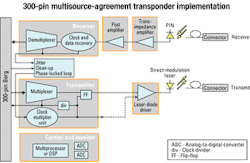
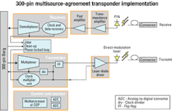
At 10 Gbits/sec, the most dominant MSA has been the 300-pin MSA. The MSA calls for receive and transmit optical interfaces for 1310- and 1550-nm wavelengths for distances ranging from 600 m to 80 km. On the equipment side, the interface is based on the Optical Internetworking Forum's (OIF) SFI-4 specification, a 16-bit parallel LVDS data and clock interface.A typical SR module is shown in Figure 1. Key components in the receive path are the PIN diode, transimpedance amplifier (TIA), post-amplifier (PA), clock and data recovery (CDR), and demultiplexer. In the transmit path, the components consist of the multiplexer, clock multiplier unit (CMU), laser-diode driver (LDD), and direct-modulated laser (DML). In a long-reach module, the LDD would be replaced with an external modulator and driver. A continuous wave or tunable laser would then be used in place of the DML. Other semiconductors in the module might include control and monitoring circuitry composed of a DSP and analog-to-digital converters.
The semiconductor components for 10 Gbits/sec have been defined around this common architecture and within the limits of integration. The parallel data interface must be compatible with the 16-bit LVDS transmit and receive data with reference clock and data clock. The internal interfaces are defined by natural integration boundaries. These may vary slightly from vendor to vendor for features that leave room for multiple implementations and as each manufacturer seeks to add value.
Receiver ICs have integrated the demultiplexer, CDR, and PA together. In spite of the PA integration into the receiver, designers often use a standalone PA to implement traditional features that until recently have not been available in other forms. These features include loss of signal, an indication that the optical-signal power has decreased below a threshold, and slice adjust, an offset to the one/zero decision threshold. Transmitter ICs include the CMU, multiplexer, and a small FIFO to compensate for off-chip clock and data phase variations.
Within the confines of the module, silicon vendors have sought to integrate the multiplexing and demultiplexing functions in a single-chip SerDes. The benefit of this integration is it would allow on-chip loopbacks to the line side as well as the equipment side. Of course, a single-chip transceiver would save valuable board space. However, that has been an elusive target. Many efforts have failed to minimize channel crosstalk and subsequently have not been able to meet SONET/SDH jitter generation specifications. But through the use of an appropriate CDR architecture, the transmitter voltage-controlled oscillator (VCO) can be made to operate at a different frequency than the CDR VCO, thus overcoming this hurdle.
One of the key benefits of the 300-pin MSA is it provides a complete optical front-end with an easily manageable interface. The data and clock operate at 622 MHz, which minimizes high-frequency printed-circuit-board (PCB) design requirements. The interface is compatible with SFI-4 and has been adopted by numerous IC vendors. This interface can support SONET/SDH, forward error correction (FEC) rate SONET/ SDH, and the 10-Gigabit Ethernet (10-GbE) XSBI interface.
However, there is a price tag associated with the 300-pin MSA. The optical interface is the most significant added value offered by the module vendor. In high-volume applications such as short-reach (SR) and very-short-reach (VSR) links, the SerDes IC becomes a significant cost factor in the price of a module. Because this expense is so significant, several companies sought a merger of semiconductor design technologies (e.g., Vitesse Semiconductor acquired Versatile Optical Networks in June 2001). Another consideration is that the SerDes is largely independent of the optics. It is included in the module to allow the end user to avoid any high-speed design associated with the 10-Gbit/sec serial interface of the SerDes.
There are two dominant module architectures that have developed following the widespread implementation of the 300-pin MSA. XENPAK and similar MSAs such as X2 and XPAK serve an emerging 10-GbE market. Meanwhile, XFP addresses economics and density while serving a broad application base. The XENPAK MSA demands additional features to support the XAUI interface, which is a 4-bit, 3.125-Gbit/sec unclocked LVDS interface. The XFP MSA trims the module down to a serial interface using a subset of the components common to both the 300-pin MSA and XENPAK specifications.
XENPAK. The XENPAK and XPAK MSA architectures are based on 10-GbE interfaces described in the IEEE-803.2ae standard. The XAUI interface was chosen because it is a low-pin-count interface that requires no clock. The bit rate for XAUI is 3.125 Gbits/sec, which can be readily implemented in standard CMOS. The data is self-aligned, meaning that the four channels are deskewed automatically by the SerDes. Even though the parallel data rate is much higher than that of the 300-pin MSA, by freeing the designer of the restrictions of clock and data phase alignment, the implementation is much simpler. This interface allows up to 20 inches of FR-4 trace, and some vendors are shipping products that support up to 40 inches of trace with either equalization or pre-emphasis.For the semiconductor vendor, there is an increased complexity in the SerDes (except in a wide WDM application). A typical SerDes is shown in Figure 2. The additional circuitry includes 64B/66B encoding and decoding for the serial side, 8B/10B encoding and decoding for the parallel side, and quad SerDes with deskew. The fundamental nature of the transceiver changes in that there is a large digital section in addition to the mixed-signal SerDes of the 300-pin MSA.
Although XENPAK is primarily a 10-GbE MSA, there is a new implementation agreement, called SFI-4 Phase 2, being considered at the OIF that supports a compatible architecture for SONET data. That would allow module vendors to offer products supporting 10.3125-Gbit/sec serial 10-GbE and 9.953-Gbit/sec SONET in a pin-compatible, identical form-factor module. One key difference is that the SFI-4 Phase 2 interface is designed for only 8 inches of FR-4 trace.
The parallel data interface for SFI-4 Phase 2 operates at 2.566 Gbits/sec per channel, corresponding to a 9.953-Gbit/sec serial data rate. When operating at 10.709 Gbits/sec, the parallel interface operates at 2.76 Gbits/sec on each of the four channels. In spite of the common pinout, the two applications require very different core circuitry in the SerDes.
In addition to providing a low-pin-count design-friendly interface, XENPAK allows a higher port density than the 300-pin MSA, up to eight ports on a typical line card. With 10-GbE the main application, low cost is a major focus for vendors and users.
Criticism of the XENPAK module has centered on the size of the module and the port density. In response, new MSAs have arisen that are pin-compatible to XENPAK's 70-pin connector. XPAK is one of these MSAs. Another group, called X2, has formed to develop a smaller module form factor based on XENPAK as well. The X2 MSA is targeted at applications needing <10-km transmit distance that will dissipate less power and thus allow a smaller size.
The X2 MSA copies freely from XENPAK, using the same optical interface, 70-pin connector, and XAUI interface. Like XENPAK, support is planned for SFI-4 Phase 2. An advantage to the semiconductor vendor is that chips developed for XENPAK will also likely support X2.
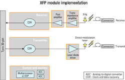
XFP. While X2 develops a half-sized XENPAK module, a more radical approach to reducing cost and size is XFP, which eliminates the SerDes from the module much as has been done with popular 2.5-Gbit/sec small-form-factor (SFF) and small-form-factor-pluggable (SFP) modules. The XFP MSA seeks to find the best solution for cost, port density, and flexibility. The XFP module provides a serial 10-Gbit/sec electrical interface to the equipment, which places the SerDes outside the module on the equipment manufacturer's line card. The module itself includes a CDR, LDD, and DML on the transmit side. On the receive side, it includes the PIN, TIA, PA, and CDR. This implementation is shown in Figure 3.In the module, functions that traditionally have been integrated with the SerDes are now standalone ICs. The XFP module will typically use two CDRs, one of which will have an integrated PA. For any given link application, the physical media devices and the optics will remain the same as in another MSA. The key value proposition of the XFP module is a combination of three factors: size, cost, and flexibility. The size will permit up to 16 ports on a single line card. XFP reduces the bill of materials to exclude the high-cost SerDes and strives to be the module of choice for high-volume short-range applications. It will also be useful for standard-rate SONET (9.953 Gbits/sec), 10-GbE (10.3125 Gbits/sec), 10-Gigabit Fibre Channel (10.5 Gbits/sec), and G.709 FEC rate SONET (10.7 Gbits/sec). It is protocol-independent, so the data format is transparent. The disadvantage of the XFP module is that the designer must handle 10-Gbit/sec data on the line card. That can add design time and require additional CAD tools and a more expensive PCB material.
Outside the XFP MSA. Perhaps more significant than the XFP MSA itself is how it will influence system design and ultimately semiconductor design. Unlike the 300-pin MSA and XENPAK MSA, there is no predetermined parallel boundary. The SerDes can be integrated with large digital ASICs such as a framer or FEC codec. Integrating these functions into a single chip will eliminate a parallel interface and save nearly 500 mW of power. There is also a natural integration of these functions that is permitted by advanced semiconductor technology.
With the exception of network monitoring, the FEC data is of no interest. It serves to detect and correct bit errors in the link. Once the data has been restored, the FEC overhead is discarded. Thus, the boundary between the SerDes and FEC is a logical interface to eliminate.
With the proliferation of MSAs, systems designers can now choose the optimum solution to meet the needs of their platform. There are many nuances that have not been addressed here that feed into the decision process. It is critical for designers to understand their core capabilities and limitations. There is no "one size fits all" for optical modules; the best solution comes from a detailed analysis.
James Doscher is director of marketing, High Speed Networking Group, at Analog Devices Inc. (Cambridge, MA).


