New optical packaging required for 10-Gbit/sectransceiver components
The development of cost-effective optical-component technology is crucial to the continued growth of the optical communications industry. Key industry trends such as standards convergence and the increasing use of optical transceivers are providing an opportunity to increase the cost-effectiveness of technology for 10-Gbit/sec applications. To make the most of this opportunity, manufacturers require a flexible approach to component-level packaging.
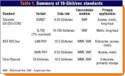
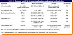
Demand for new optical packaging is partly driven by the fact that three important industry standards converge at a data rate of approximately 10 Gbits/sec. These standards are Telcordia GR-253-CORE (OC-192) (and the related ITU-T G.691 SDH [STM-64] and ITU-T G.709 optical transport network standards); IEEE 802.3ae 10-Gigabit Ethernet standard; and the 10-Gbit/sec version of the Fibre Channel standards. Although each standard prescribes slightly different data rates and formats, the requirements are close enough that all will use similar optical-component technology, as shown in Table 1.As a result, it will be possible to use common serial 10-Gbit/sec optical technology platforms to meet the requirements of all the standards. By combining the volumes from several different applications, component manufacturers will be able to reduce costs and upgrade equipment performance from lower data rates.
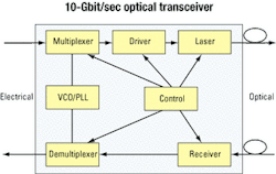
An important trend emerging for 10-Gbit/sec components is the use of modules that integrate optical transmit and receive components with high-speed electronics. These devices, known as optical transceivers, are common in 1-Gigabit Ethernet and 1- and 2-Gbit/sec Fibre Channel applications. Until recently, OC-48 (2.5-Gbit/sec) and OC-192 (10-Gbit/sec) SONET line cards were built from discrete optical and high-speed electronic components. Over the last two years, several multisource agreements (MSAs) for 10-Gbit/sec transceivers emerged (see Figure 1), and the use of these MSA-compliant modules to replace discrete component implementations is increasing dramatically.Applications generally require different optical power budgets and dispersion parameters to meet the reach requirements of the fiber links. To fulfill the comprehensive set of application requirements, several different types of lasers and receivers are required.
Vertical-cavity surface-emitting lasers (VCSELs) operating at 850 nm are used in very-short-reach (VSR) transceivers for multimode-fiber applications in the enterprise market. Fabry-Perot (FP) or distributed-feedback (DFB) lasers operating at 1310 nm are commonly used in VSR and short-reach (600-m-20-km) singlemode-fiber applications for access and box-to-box connections. Typically modulated by turning the laser on and off, these types of lasers are referred to as directly modulated lasers. Long-wavelength (1310-nm) VCSELs are also under development and will provide a cost-effective alternative to edge-emitting lasers if key performance parameters can ultimately be met.
Until recently, 10-Gbit/sec FP and DFB lasers used thermo-electric coolers (TECs) to keep the lasers at modest operating temperatures (35°C or less) to meet their performance and lifetime requirements. Unfortunately, TECs increase costs, are often unreliable, and draw significant power during high-temperature operation. Today, DFB lasers have emerged that can operate without coolers and still meet performance and lifetime requirements.Although the packaging and control challenges are in some ways more severe, uncooled lasers have a significant advantage over cooled lasers because of their lower power draw when operating at high temperatures.
Electro-absorptive modulated lasers operating at 1550 nm are typically used for intermediate-reach applications (25-40 km). These lasers consist of a DFB laser monolithically integrated with an externally modulated electro-absorption (EA) section. For more demanding applications and longer reaches, the EA section of the device can be optimized if it is individually fabricated as a separate chip and then co-packaged with the laser chip. Unfortunately, while cost-effective, the modulators in these lasers have narrow spectral widths, and optical output powers are limited by the relatively high loss through the EA sections. Therefore, DWDM systems and long-reach (80-km) applications require a combination of a high-power DFB laser and low-loss Mach-Zehnder interferometer modulator.
Receiver technology is somewhat simpler, since only two types of photodiodes are used: p-intrinsic-n (PIN) for the shorter-reach applications and avalanche photodiodes (APDs) for the longer-reach applications. PIN receivers typically provide lower gain per photon and are less expensive than APD receivers due to their simpler structures. An important benefit to PINs is their lower susceptibility to optical overload conditions. In most applications, high-performance, overload-resistant PIN receivers can be used "back-to-back" (i.e., with a very short fiber link) and still function properly. APD receivers, on the other hand, can become saturated or damaged by even modest input optical powers. With short fiber links, optical attenuators must be used in front of the APD receiver.
A final important trend, particularly in long-haul and metro telecommunications applications, is the use of tunable lasers. Tunable lasers provide three primary benefits to the user relative to fixed wavelength lasers:
- Reduction of logistics and inventory costs related to planning, procuring, and sparing lasers or cards with unique wavelengths.
- Decreasing the time to provision a new channel by providing a "universal" line card that can be turned on, tuned, and locked to the desired channel in a matter of seconds.
- In the longer term, providing a means to dynamically provision, add/ drop, and/or restore wavelengths remotely and automatically.
The implementation of high-power, broadly tunable lasers could be one of the more important new features of next-generation optical networks.
For the optical-component manufacturer, the diversity of applications in the 10-Gbit/sec market requires a flexible approach to component-level packaging that applies to both laser and receiver modules and addresses the emerging need for tunable lasers. Key challenges in the development of a comprehensive packaging approach include the following:
- Ability to precisely align the laser chip or photodiode to singlemode fiber with high coupling efficiency and maintain this alignment throughout the lifetime of the product, as demonstrated by meeting Telcordia and other reliability requirements.
- Creation of a flexible platform that applies to a number of different products and applications, without the need to redesign the package for each new component.
- Ability to meet the radio-frequency (RF), thermal, and hermetic-sealing requirements of 10-Gbit/sec components and provision for integrating these components directly into the package for cost, space, and power savings.
- Simultaneous development of a low-cost automation capability that allows the manufacturing to be scaled to meet the anticipated growth and cost requirements of the market.
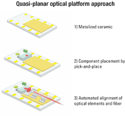
The quasi-planar optical platform1,2 is based on a metallized ceramic substrate and microflexure alignment principle (see Figure 2). Module assembly begins with a ceramic substrate (designed for use with very-high-speed components) and high thermal dissipation capabilities. Optical chips (lasers, photodiodes, monitoring diodes) and electronic components (laser drivers, transimpedance amplifiers, RF matching circuitry) are mounted on the ceramic by pick-and-place techniques commonly used in the electronics industry. The components are affixed to the substrates using fluxless soldering processes within about 10 microns of accuracy. The pick-and-place automation can use relatively simple, rapid machine vision for accurate placement, since the substrate is planar and the optics will be aligned actively in the next step.
Other optical components such as lenses, isolators, and metallized fibers are pre-assembled on flexible metallic elements called microflexures. The pre-assemblies are then placed in coarse optical alignment on the ceramic platform, again using machine vision. Fine alignment is obtained by slightly deforming the flexure in an automated process using an active-mode system to provide feedback on the alignment.
After alignment, the flexure is laser-welded to a metallic weld plate on the ceramic. The flexure is designed to maintain the alignment after welding, even over severe temperature excursions, mechanical stresses, and the lifetime of the product. To complete the package, the optical subassembly can be mounted in a butterfly can, the high-speed circuits wire-bonded to the leads of the can, and the lid and fiber feed-through sealed to create a hermetic enclosure.
Conventional butterfly cans are well known and reliable but relatively bulky and expensive. A higher-performance and more cost-effective enclosure is realized if a multilayer high-speed ceramic substrate serves as both the interconnection platform and the floor of the package. By using a high thermal conductivity material, the platform is very useful at dissipating the heat of uncooled laser chips and can incorporate unpackaged driver chips.
In this "mini-module," the pins of the package are an integral element of the platform, and high-speed 10-Gbit/sec differential input/output pins are placed directly at the end of the package, opposite to the fiber. The low-speed connections are placed on each side of the package for convenient surface-mount soldering and RF access. High-speed signals are routed inside the planar multilayer ceramic with controlled impedance and connected to a submount assembly placed on the top surface of the ceramic.
Optical elements, including a specially designed isolator assembly, are then automatically placed, aligned, and welded to the metallic top of the substrate using flexures. A custom-designed pick-and-place and alignment machine uses a combination of machine vision and active feedback to complete the singlemode-fiber alignment. Laser-welding technology is used to fix the flexures to the substrate once the alignment is completed. To complete the package, a cap is placed over the whole assembly and hermetically sealed around the edges of the substrate.
The completed miniature package has a footprint of only 9×16 mm. This package design has been successfully used to create an uncooled 10-Gbit/sec DFB laser module, including integrated driver, and 10-Gbit/sec PIN and APD receiver modules.
These mini-modules can be surface-mount assembled. The high-speed differential output enables excellent signal integrity in connection with 10-Gbit/sec multiplexing and demultiplexing chipsets. The integrated chip driver allows a lower-impedance, high-speed interface, which saves power, space, and cost relative to conventional laser modules used with external packaged drivers.
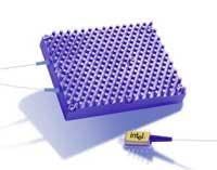
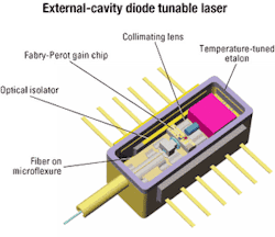
The miniature modules enable the creation of small-footprint transceivers featuring uncooled lasers and high-performance PIN or APD-based receivers. The laser and receiver modules are integrated with various high-speed electronic chips to create optical transceivers based on the specifications listed in the 300-pin MSA (see Photo) or in the XENPAK module MSA.The quasi-planar optical platform approach works especially well for assembling tunable-laser modules (see Figure 3). The laser design comprises an external-cavity diode laser (ECDL) wholly mounted on a ceramic platform placed on a TEC within a 14-pin butterfly-type package. The ECDL tunable laser features high output power (20 mW) and integrated wavelength locking and is tunable across the full C- or L-bands. It uses a novel etalon-based widely tunable filter to achieve singlemode operation at selectable wavelengths.3
There are no moving parts in this type of tunable laser. As a result, the laser is not susceptible to shock and vibration issues inherent in other types of widely tunable lasers.Quasi-planar packaging is well suited to the high-volume manufacturing of optical components for the emerging 10-Gbit/sec transceiver market. Packaging technology must be flexible enough to accommodate a variety of laser and receiver types. The trend toward small-footprint transceivers is creating requirements for packages that house uncooled lasers and more high-speed electronics. In the near future, tunable lasers will emerge that rely on complex yet low-cost packaging to meet aggressive cost targets demanded by this market segment.
The flexible automated quasi-planar optical platform can be used to create a variety of components, including uncooled laser modules with integrated drivers, high-performance PIN and APD-based receivers, and external-cavity tunable lasers.
Gary H. Wiseman is director of marketing at the Optical Platform Division and Jean-Marc Verdiell is an Intel fellow and director of the Optical Technology Office at Intel (Newark, CA).
- "Automated Opto-Electronic Packaging for 10 Gb/s Transponders," J.-M. Verdiell, et al., 51st Electronic Components and Technology Conference proceedings, Buena Vista Lake, FL, May 2001, pp. 429-432.
- "Automated Optoelectronic Manufacturing for 10 Gb/s Transponders," J.-M. Verdiell, et al., Proc. SPIE Photonics West proceedings, San Jose, CA, January 2002.
- T. Bodenhamer and J.K. Lee, "Meeting future growth and service requirements with high-performance, widely tunable lasers," Lightwave, March 2002, p. 142.

