Nanofabricated isolators address low-cost FTTH
The fiber to the home infrastructure necessary to meet consumer demands for voice, data, and video has fueled the growth of transceiver sales over the last year. Transceiver vendors have responded to the cost pressures demanded for these applications with design innovations and improved manufacturing efficiencies.
However, further innovations in device miniaturization, subcomponent integration, materials utilization efficiency, and reduced power consumption are required to achieve even lower costs if high-bandwidth services are to become widely deployed. To date, significant resources have been expended on reducing the costs of many transceiver subcomponents and simplifying the integration of the subcomponents into the transceiver. Yet, optical isolators have changed little over the years, and the process of integrating isolators into the transceiver remains as complex as ever.
The optical isolator, a subcomponent placed between the laser and fiber stub to protect the laser from surface reflections in the optical network, is a limiting subcomponent in the transceiver’s laser module that can consume up to 20% of the module’s optical length. The size and thickness of the isolator also limits the coupling optics, putting additional cost constraints on the module design. Reducing the size and/or thickness of the isolator can significantly improve the transceiver packaging and give optical designers more flexibility to reduce costs. Nanofabricated optical isolators address this need; they have significant advantages over traditionally manufactured isolators that radically reduce the acquisition and integration costs needed for broadband services distribution.
Traditional single-stage polarization-dependent optical isolators are manufactured by assembling discrete polarizers on either side of a rare earth, iron-garnet Faraday rotator. The assembly can be done with epoxy (lamination) to minimize labor costs or epoxy-free to minimize material costs. The polarizers used in current isolator designs are manufactured through a glass melting, doping, and stretching process with inherent limitations that limit the size and thickness of the discrete polarizers, increasing the thickness of the isolator by as much as 130%.
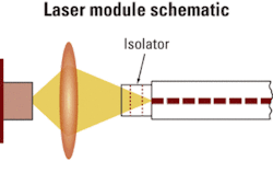
After assembly of the discrete polarizers to the Faraday rotator, the isolator wafers are generally 11×11×0.7 mm thick for 1310-nm applications or 11×11×0.9 mm thick for 1550-nm applications. The thickness of the isolator, together with transceiver-design parameters and laser-module constraints, limit how small the isolator can be. And because manufacturing yields go down significantly as the ratio of the height to the width of the isolator exceeds 1:1, isolator thickness has an economic impact. As a result, most isolators used in today’s transceiver designs are 1-1.2 mm on a side, and ~100 isolators can be manufactured from a wafer. Reducing the thickness of the isolator would enable smaller isolators to be manufactured without reducing dicing yields, eliminating a key impediment to further cost reductions.A schematic of a typical laser module is shown in Figure 1. Light from a laser diode is coupled into a fiber stub by one or more focusing lenses. The distance between the lens and fiber stub is generally small and fixed by the transceiver-design architecture, which likewise constrains the numeric aperture (NA) of the focusing system.
Surface reflections in the optical network can cause mode and/or wavelength switching in single-frequency lasers (DFB, VCSEL, etc.), causing increased noise in the transmitter or outright failure of the laser module. An optical isolator protects the laser from these surface reflections, and the thickness of the optical isolator together with the NA of the coupling system dictates the physical dimensions of the isolator. In other words, the thicker the isolator, the larger the dimensions must be for efficient coupling of the focused light into the fiber stub.
To eliminate the constraints on the laser module imposed by the isolator, the isolator itself must be manufactured thinner than conventional technology allows. Nanofabrication is a disruptive technology that overcomes this technology hurdle and enables smaller isolators to be manufactured, thus maintaining the system NA and simultaneously increasing the number of isolators that can be manufactured from a single wafer.
Nanofabrication is the manipulation of optical material on a submicron scale.1 With the appropriate selection of materials and structural shapes and sizes, a wide variety of optical functions, called nano-optics, can be manufactured.2 Numerous nanofabricated optical components are commercially available today, including polarizers, polarization beamsplitters, phase retarders, and optical filters.2 Nanostructures can also be integrated with other optical components to create more complex optical functions in a very thin form factor.3 An optical isolator can be manufactured by integrating polarization nanostructures onto a Faraday rotator.3,4,5
Polarization nanostructures are constructed from an array of metallic “wires” with a periodicity significantly less than the wavelength of the incident light. The metallic wires act as a dielectric for light that is polarized perpendicular to the array and allow the light to be transmitted. Light polarized in the orthogonal direction is blocked, since the wires act as a conductor. The total thickness of all layers of a polarization nanostructure is less than a micron thick, so a carrier substrate is required for a support structure. A standard material such as BK 7 is used as the carrier substrate for discrete polarizers; however, monolithically integrated nano-optics use a judiciously chosen carrier substrate with its own optical functionality.
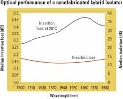
For example, placing polarization nanostructures directly on a Faraday rotator carrier substrate forms an optical isolator whose thickness can be reduced to that of the garnet substrate itself. Nanofabricated isolators can be manufactured with polarization nanostructures replacing one discrete polarizer (hybrid isolators) or both discrete polarizers (monolithic isolators). The hybrid isolators available today reduce the total isolator thickness by 20%-30%, which in turn enables the size of the isolator to be reduced by 40%-50% (maintaining a fixed height-to-width ratio). As a result, more than 300 isolators can be manufactured from a hybrid isolator wafer, a three-fold increase over traditional manufacturing processes. The optical performance of hybrid isolators is comparable to conventionally manufactured isolators (see Figure 2) but with a significantly reduced form factor.Nanofabricated isolators incorporate a visual alignment aid that simplifies integration in the laser module. A traditionally manufactured isolator has no clear visual clues to enable the input side of the isolator to be distinguished from the output side, nor is the orientation of the input polarization easily identifiable. To ease the integration of the isolator into the laser module, manufacturers must resort to a marking scheme to clearly identify the isolator’s orientation. The marking scheme can be in the form of a physical mark on the isolator, adding more handling processes and cost. More commonly the isolator is diced to a rectangular aspect ratio that allows a quick identification of the polarization orientation, reducing the isolator yield from each wafer and increasing the per-unit cost. The smaller the isolator, the more magnified the challenges associated with identifying the isolator orientation-and thus the greater the cost.
Nanofabricated isolators eliminate the problem of the orientation mark by encoding an artifact into the polarization nanostructure that is observable through a simple polarization filter. Such a filter can be easily and inexpensively incorporated into a laser-module manufacturing line. When viewed through the polarization filter, the polarization axis “pops out” in vivid color, identifying the direction of input polarization. This artifact further reduces integration costs by eliminating the need for a post-processing axis identification and marking procedure.
Nanofabricated hybrid isolators are currently manufactured using both latched garnet and non-latched garnet substrates. Individual isolators utilizing latched garnet Faraday rotators have completed environmental qualification testing and are in full commercial production, shipping to transceiver vendors today. Wafers of nanofabricated hybrid isolators utilizing non-latched garnet Faraday rotators (isolator cores) are beginning commercial sampling to isolator manufacturers and contract manufacturers.
Nanofabricated monolithic isolators will augment nanofabricated hybrid isolators within the next year, yielding nearly 700 isolators from a single wafer, a seven-fold increase over the quantities realized with traditional manufacturing processes in use today. This innovation will enable optical isolators to cross the $1 barrier and help enable CWDM in metro and access networks to become widely available.
Further, the current size of the isolator wafer is limited by the size of the garnet; nanofabrication processes can easily process substrates with a 4-6-inch diameter. When larger Faraday rotator substrates become available, still more significant price reductions will be attainable. As a result, nanofabricated optical isolators will continue to enable transceiver manufacturers to achieve savings of millions of dollars per year and expand their markets in support of the emerging requirements for high-bandwidth solutions.Alan C. Graham is sales development director and Jian Jim Wang is chief technology officer at NanoOpto (Somerset, NJ).
1. H. Kostal, J. Wang, “Nano-Optic devices enable integrated fabrication,” Laser Focus World, pp. 155-159, June 2004.
2. J.J. Wang, L. Chen, S. Tai, D. Deng, P. Sciortino, J. Deng, F. Liu, “Wafer based nano-structure manufacturing for integrated nano-optic devices.” Journal of Lightwave Technology, Vol. 23, No. 2, February 2005.
3. J.J. Wang, J. Deng, X. Deng, F. Liu, P. Sciortino, L. Chen, A, Nikolov, A. Graham, “Innovative high-performance nanowire-grid polarizers and integrated isolators,”IEEE Selected Topics in Quantum Electronics, Vol. 11, No. 11, pp. 241-253, January/February 2005.
4. J.J. Wang, X. Deng, L. Chen, P. Sciortino, J. Deng, F. Liu, A. Nikolov, A. Graham, Y. Huang, “Innovative nano-optical devices, integration and nano-fabrication technologies,” Proceedings of SPIE,Vol. 5623, pp. 259-273, 2005.
5. J.J. Wang, L. Chen, S. Tai, X. Deng, P. Sciortino, F. Liu, J. Deng, X. Liu, A. Nikolov, D. Sinatore, “Nano-optical devices and integration based on nano-pattern replications and nanolithography,” Proceedings of SPIE,Vol. 5592, pp. 51-62, 2005.


