Novel wafer-level packaging approaches attract funding
While funding for optical companies remains difficult to come by, two startups have managed to raise money based on their wafer-level approaches to functional integration. Both ASIP (Somerset, NJ) and Xponent Photonics (Monrovia, CA) promise lower costs and smaller footprints via their laser and receiver technologies.
ASIP closed $16 million in the initial installment of its Series C financing round from Nokia Venture Partners, Finaventures, Intel, and Redpoint Ventures in July. As reported previously (see Lightwave, December 2002, "Startups pursue wafer-level integration," front page), ASIP relies on a technique it has dubbed Asymmetric TwinGuide (ATG) to integrate passive and active functions within the same indium phosphide (InP) wafer growth. While most integration approaches combine functions laterally, ATG integrates them vertically. For example, the laser source may be on one layer and the laser's modulator may be on the layer below. The company exploits asymmetry between the refractive indices to enable the light to propagate from one layer to the other via a taper etched into the layer containing the laser source; the taper acts as a concentrator and a mode transformer.
"We're taking the complexity out of the growth, which traditionally is where it has been, and putting it into processing," explains Yassi Moghaddam, marketing vice president at ASIP. "Processing complexity has been pretty much mastered over the last 40 years through semiconductor processing."
The company has begun sampling chip and chip-on-submount versions of an uncooled 1310-nm electro-absorption modulated laser (EML)/modulator combination as well as "semi-cooled" 1550-nm devices. Moghaddam expects 1310-nm components in TOSA packages to become available in sample quantities this year, with volume quantities available in the first half of next year.
At least one of those samples ended up at Ignis Optics (San Jose, CA); the transceiver manufacturer displayed a 1310-nm XFP using ASIP's EML at OFC last March. The XFP demonstration was not a coincidence. "XFP sets the bar for cost, for power dissipation, and for form factor," says Moghaddam. "So if you design something that meets XFP requirements, by definition it would meet other form factors' requirements."
Vendors of short- and intermediate-reach transceivers represent the company's main target for the 1310-nm devices, Moghaddam says. While the emerging 10-Gbit/sec Ethernet groups like XFP, X2, XPAK, and XENPAK are natural applications, Moghaddam reports that vendors of SONET/SDH devices such as 300-pin transceivers also have shown interest in ASIP's technology.
The new funding will enable the company to support its tier one customers as well as complete its product line. That includes the 1550-nm product family. The company has delivered samples of its 40-km devices and expects them to reach general availability in the first quarter of next year. The second half of 2004 should see the introduction of 80-km and WDM versions. The company describes the 1550-nm sources as semi-cooled because the device has an operating window of 50°–55°C and therefore does not require the cooling level of other 1550-nm lasers. In both the 1310- and 1550-nm product lines, the company will emphasize its low-cost packaging, which enables the use of the TO-cans common to lower-speed devices. The ASIP devices also offer low power dissipation—for example, 2.1 W of power dissipation for the 1310-nm device in 7-km SR-1 and 10-km 10-Gigabit Ethernet applications and 3.4-W dissipation for the 40-km 1550-nm component. They also do not require monitor photodiodes.
Meanwhile, Xponent Photonics also has secured C round funding, although the amount had not been released at press time. Low-cost packaging is the company's calling card as well; it uses a technology the company calls Surface Mount Photonics (SMP), which combines planar-lightwave-circuit (PLC), active, and passive expertise to eliminate custom assembly equipment, labor, and overhead. According to Teresa Englehard, the company's vice president of marketing, SMP enables passive alignment, flip-chip assembly, and wafer/bar-level test and burn-in but does not require hermetic packaging, thus reducing costs significantly.
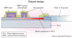
The heart of the SMP technology resides at the wafer level. Instead of using the cleaved facets common to edge-emitting lasers, Xponent's design uses vertical etched facets in an InP structure for the laser mirrors. The light from the active portion couples into a passive dielectric waveguide that is deposited on the front section of the laser chip. During packaging, the device is flipped upside down and coupled to a mating waveguide on the PLC (see Figure). The result, says Englehard, is nearly 100% power transfer with a lateral alignment tolerance exceeding ±2 microns—within the capabilities of current semiconductor bonder systems. Fiber is attached to the device via a V-groove in the PLC.Because the light as well as other electrical contacts to the laser or other active devices is not exposed to air, the SMP device does not need to be hermetically sealed. As illustrated in the Figure, an "encapsulant" is used instead.
The company will use SMP chips as the basis for what it calls "fiber-ready optical assemblies" (FROAs) as well as traditional optical assemblies such as TOSAs and ROSAs. Like ASIP, Xponent sees transceivers as a ready market for its technology. Its first product is a 10-Gbit/sec PIN photodiode FROA, which it has priced at $10 apiece in volume. The component offers 1-A/W typical responsivity at 1550 nm. In addition to the FROA version, fiber-fixed versions are planned in receptacled and pigtailed TO-can-compatible packages. Meanwhile, a Fabry-Perot TOSA is expected to debut this month.
Englehard says Xponent also sees a future in the fiber to the premises market. The company has a triplexer FROA on the drawing board that is significantly smaller than a dime. The assembly requires seven piece parts (not including the fiber details) and one-fifth the labor hours necessary to construct a traditional device. The company expects to unveil the triplexer by the end of this year.

