CMOS photonics is here
On rare occasions a new technology emerges that has a profound impact on how we communicate and build communication networks. In some cases the new technology offers incremental improvement and does not require significant changes to network infrastructure. In other cases, a new technology brings dramatic improvements in cost and performance, but it requires a mindset shift to facilitate its deployment. Transition from analog to digital technologies, from copper to fiber, and from wired to wireline technologies can be placed in the category of such historical shifts. Today we are on the verge of another such breakthrough, brought to us courtesy of CMOS photonics.
CMOS photonics has been in a research state for the last few years with a goal of evolving photonics to the same level of integration, low power, and low cost traditionally associated with CMOS electronic circuits. Historically, we see a dramatic transition from the individual transistors prevalent in electronic circuits prior to the 1950s, to the primitive integrated circuits of the 1960s, to today’s very large scale integration (VLSI) chips composed of millions of transistors. This transition has been described by Moore’s Law, which states that the number of transistors on integrated circuits (a rough measure of computer processing power) doubles every 18 months.
Photonics has not enjoyed the technological and cost-efficiency progress that silicon has. Today’s optical modules consist of discrete lasers, photodetectors, and associated electronic elements built into transmit optical subassemblies (TOSAs) and receive optical subassemblies (ROSAs). These subassemblies are in turn assembled on small circuit boards along with dozens of discrete electronic elements to create an optical module such as an XFP or SFP (see Photo 1). These difficult-to-manufacture modules exhibit low final test yields and poor reliability, resulting in high ASPs and operational costs. A short-reach 10-Gbit/sec XFP module currently sells for just under $300 in volume to OEMs. End users are often faced with significant markups on top of this price.
With CMOS photonics entering commercialization, this situation no longer needs to apply. CMOS photonics integrates all optical and electronic elements necessary to build an optical transceiver on a monolithic CMOS die. Photonic elements communicate with each other via optical waveguides etched directly on the same die as the electronic circuits that are communicating via traditional metallic interconnect.
On the receive side, the device translates photons into electrons; the opposite occurs on the transmit side. A direct current (DC) electric power supply is applied to the circuit to power the electronics while a continuous wave (CW) laser light source is applied to photonic circuits to provide optical power. Today standard CMOS cannot generate light; thus, an indium phosphide (InP) laser is attached directly to the surface of the die. Once in a waveguide, light is modulated using photonic devices such as a Mach-Zehnder modulator to achieve the on/off binary signaling.
One of the key challenges of CMOS photonics is to get the light on and off the die. Early implementations tried to do this from the die’s edge. In this approach, a wafer must be cut, each die edge polished, and an antireflective coating must be deposited on the sidewall of the die. After that, the device must be at least partially assembled in a package before it can be tested for the first time. Although working devices can be built this way, the yield is low and, as a result, individual component costs are high-which renders this approach unsuitable for high-volume commercial applications.
Thus, a better way of getting the light on and off the die-preferably from the surface of the die-is necessary to reach the economies of scale traditionally associated with electronics. Such an approach would have numerous benefits. A die could be fully tested optically and electrically using standard wafer testers equipped with electrical and optical probes. Good die could be marked and used for packaging, resulting in high production assembly and test yields. Lasers could be passively aligned and attached to the surface of the die to provide a light source to the photonic circuits. Light from a receive fiber could be brought onto a chip and converted to electrons using embedded photodetectors.
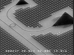
The optimal method to get light on and off a die in this way is to use a holographic lens. The lens expands the size of the optical mode from a waveguide into a larger surface area closely matching the planar area of a fiber. As light impinges on the lens from the silicon waveguide, it is scattered normal to the plane of the die and into the fiber. By the time the light reaches the far end of the holographic structure all of it is directed into the fiber.
The challenge is to achieve such a holographic feature in a standard CMOS wafer factory flow. Photo 2 shows an implementation that meets this requirement.
This type of coupler makes CMOS photonics commercially feasible, but it also places certain physical restrictions on how CMOS photonics can be deployed. There are three key elements that must be understood for effective implementation of CMOS photonics in networks.
The first constraint is the fact that CMOS is transparent to light at wavelengths longer than 1,300 nm, with the most optimal coupling efficiency achieved at around 1,500 to 1,600 nm. Thus, longer optical transmission wavelengths must be used for fiber communications using CMOS photonics transceivers. The closest standard wavelength in this range is 1,550 nm, a wavelength that traditionally has been used in long-haul networks. With the economies of CMOS photonics, however, this wavelength can now be cost-effectively applied to shorter-reach metro, enterprise, and data center applications.
The second key constraint is the fact that a holographic lens’ surface area must closely match the cross-sectional area of the fiber. Since the cross-section of singlemode fiber is about 50× smaller than that of multimode fiber, singlemode fiber is most suitable to CMOS photonics applications. The additional benefit of singlemode fiber is that it costs less per meter than multimode fiber-a fact that is perhaps not well known in the optical industry.A better approach is to use an MT-RJ or MTP-style connector, both of which are already widely used in fiber-optic communications. Optical fiber cables with preconnected MT-style connectors can be readily purchased at many lengths or can be field attached using off-the-shelf tools.
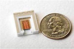
Research into the issues described previously has culminated in the first fully monolithic 10-Gbit/sec transceiver in a 0.13-µm standard CMOS SOI process. The possibilities are many. For example, sample devices that contain two XFP-equivalent transceivers on a die in a single package have been produced; they prove the feasibility of attaining the type of high-level photonic integration historically found only in electronic circuits. With CMOS photonics, Moore’s Law can now be applied to both electronics by increasing transistor density and to photonics by increasing the number of WDM wavelengths supported on the same CMOS die.Photo 3 shows the two fully integrated XFP transceivers on a single die. The package size is smaller than a quarter and the per-port size of transceivers using this technology will be less than 25% of a traditional XFP module size. CMOS photonics becomes more cost-effective with higher port counts; common cost drivers such as packaging, attachment elements, and attachment and test processes can be leveraged across more ports. This approach has the potential to drive per-port costs to less than 25% of equivalent single-XFP-based designs.
Since CMOS photonics transceivers are implemented in standard-flow, low-cost fabrication processes that are also well suited for digital circuitry, discrete optical transceivers are just the first stage of the CMOS photonics revolution. In the not very distant future, one can imagine single-chip devices containing multiple high-speed transceivers alongside millions of digital gates-thus eliminating an optical module or transceiver completely as a standalone component on a circuit board for system-to-system communications. This will be followed by optical chip-to-chip and perpetuating even to on-chip communications.
Commercial transceivers based on CMOS photonics technology will begin deliveries in 2007. So the time is coming to toss the TOSA/ROSA-based, bulky, high-cost optical modules and switch to CMOS photonics-based transceivers that operate over low-cost singlemode fiber using 1,550-nm wavelengths.
Marek S. Tlalka is vice president of marketing at Luxtera Inc. (www.luxtera.com).


