40-Gbit/sec components: drivers, issues, and solutions
Unique issues pertaining to 40-Gbit/sec transmission will require the development of new components.
JOHN FRITSCHEN and STAN LUMISH, JDS Uniphase
As optical networks move toward 40-Gbit/sec systems, designers face many issues in both the optical and electronic domains. In the optical domain, the most severe challenge is the span limits imposed by minimum optical signal-to-noise ratio (OSNR) and signal distortion. Amplifier noise, non-return-to-zero (NRZ) modulation, and electronic noise at 40 Gbits/sec create span limits that are far shorter that those at 10 Gbits/sec. Similarly, distortions caused by chromatic dispersion and polarization mode dispersion (PMD) reduce the effective transmission of 40-Gbit/sec signals.
Electronic issues at 40 Gbits/sec include the material limitations of current optoelectronic components such as signal generators, modulators, and receivers. Similar material issues exist in the design of electronic multiplexing and demultiplexing chipsets (which may include transimpedance amplifiers [TIAs], framers, and clock and data recovery [CDR]). Finally, 40-Gbit/sec electronic packaging requires high levels of integration and more compact physical implementation than at 10 Gbits/sec.
Together, these issues present a formidable set of challenges and may induce some network designers to take another look at a 25-GHz DWDM solution. However, there is a growing list of 40-Gbit/sec components that satisfactorily address these issues and provide the opportunity for systems designers to complete first-generation systems. Additionally, there are many efforts under way in the components supply community to develop 40-Gbit/sec components using new materials and new processes, and at levels of integration that will greatly improve performance.
In late 2001, several firms will demonstrate 40-Gbit/sec systems with general availability beginning in mid 2002. It is clear that 40-Gbit/sec systems, enabled by key components, will form a significant part of the network in the future. This article addresses the significant performance issues for 40-Gbit/sec systems and details the proposed component solution for each area.
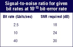
In optical-network systems, a high OSNR is the primary contributor to low bit-error rates. Therefore, system designers attempt to maximize the optical signal while minimizing the system noise. In traditional optical networks, there is a maximum in fiber power (threshold power) that can be used and not induce non-linear optical effects, such as Brillouin scattering and four-wave mixing. The maximum power is set for both intial launch and subsequent amplifier stages, and is independent of bit rate.However, network noise is directly correlated to bit rate, since the receiver collects all optical and elctronic noise from almost DC to the design bit rate. Therefore, a 40-Gbit/sec receiver will experience 6 dB more noise than a 10-Gbit/sec and 12 dB more than a 2.5-Gbit/sec receiver. Table 1 shows the SNR for a typical 0.1-nm optical bandwidth. (Note these results include about 9 dB of system margin for temperature, aging, noise, inter-symbol interference, and finite extinction ratio. These numbers are empirical.)
The following is an example of OSNR that is required in a sample operating at 40 Gbits/sec. The simplified governing equation for SNR in this type of system is:
SNR=58-10xlog10(MxN)-Lspan-NF+Ptor+GRaman-R.
Assume five 100-km spans with 25-dB loss per span (Lspan). The number of optical amplifiers is six (N, including post- and preamplifiers). The number of channels is 32 (M, which assumes L-band on 200-GHz spacing), 6 dB is the noise figure (NF), 23 dBm is the optical amplifier output power (Ptot), and there is 10 dB of Raman gain (GRaman) and 0.5 dB of ripple (R, assuming the ripples add up). These numbers lead to an SNR of 33.6 dB. Note that the difference between needed and delivered SNR in this example is only 3.6 dB, which is a small margin.
Comparing the SNR needed with what is delivered, it is clear that Raman amplification is desirable because of the gain with very little additional noise compared to erbium-doped fiber amplification. (Raman amplification is similarly used to overcome SNR deficits in ultra-long-haul systems.) In addition, extremely low per-amplifier ripple over a wide optical bandwidth is required. This condition leads to the need for dynamic gain equalization across the optical band.
In addition to OSNR sensitivity, 40-Gbit/sec systems are susceptible to signal distortion. The distortions can arise from a number of sources, the most common being chromatic dispersion and PMD. Chromatic dispersion occurs because the speed of light in optical fiber is wavelength dependent; as optical signals have a finite bandwidth, a pulse-shaped distortion results.
The practical dispersion limit is inversely proportional to the square of the bit rate. At 10 Gbits/sec the limit is 1,200 psec/nm, which corresponds to 70 km of standard singlemode fiber. But at 40 Gbits/sec the limit is only 75 psec, which corresponds to 4.4 km of singlemode fiber (SMF) and about 19 km of non-zero dispersion-shifted fiber (NZDF). With a desired transmission distance of 500 km, the total dispersion would be 8,500 psec/nm in SMF and about 2,000 psec/nm in NZDF. Therefore, there can be only small errors in the dispersion compensation, about 1% in SMF and 4% in NZDF.
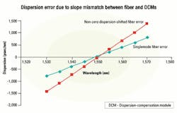
The dominant method of dispersion compensation is via dispersion-compensation modules (DCMs), which are made from spools of fibers with a large negative dispersion. However, using DCMs to compensate for the dispersion in transmission fiber induces a series of additional issues such as uncorrected (residual) dispersion and dispersion slope mismatch/error. First, since DCMs come in discrete values (170 psec/nm), there is typically some residual dispersion between ±85 psec/nm. In a 500-km link, this dispersion is of the order of 1% error for SMF and 5% for NZDF. Second, there is also an error due to the dispersion slope mismatch. The slope of SMF is 0.05 psec/nm2-km, 0.11 psec/nm2-km for NZDF, and -0.3 psec/nm2 for DCMs. That leads to substantial mismatch at the red and blue ends of the C-band spectrum for a 170-psec/nm value as illustrated in Figure 1.
In this illustration, the error is up to about 1,400 psec/nm (or 47%) for NZDF and about 800 psec/nm (about 9%) for SMF. There is also slight temperature dependence to chromatic-dispersion in fiber. So due to all the errors, tunable dispersion compensation is essential at 40 Gbits/sec. (Note that, even in a single span of 100 km, the DCM error is ±40 psec, which is already too large for 40-Gbit/sec transmission.)
Like chromatic dispersion, PMD causes distortion of the optical signal. PMD arises from the fact that all fiber has a slightly elliptical cross-section and is therefore slightly birefringent. Additionally, network modules for DWDM and optical add/drop multiplexers can exhibit a slight degree of birefringence, as can connectors and other components. Also, the magnitude of the birefringence can change slowly over time due to temperature effects.
In the case of SMF, the birefringence is specified between 0.5 and 2 psec/ √km , with the newer fibers specified at 0.5, but averaging 0.1 to 0.2 psec/ √km of PMD. Given a 500-km link, that translates into 2 to 4 psec of PMD. As the 40-Gbit/sec pulse duration is 25 psec for NRZ and shorter, say 15 psec, for return-to-zero (RZ) format, this amount of PMD represents 8 to 16% of the pulse for NRZ and 13 to 26% of the pulse for RZ. So PMD compensation will be required for any significant span of SMF and for newer fiber types any span over 500 km.
The packaging of 40-Gbit/sec electronic transitions from one component/module/part to another is particularly challenging. Not only must transmission line impedance be closely matched, but also electric field lines need to be aligned and matched through each transition. Radio frequency parasitic effects are much more difficult to control at 40 Gbits/sec in board design and chip interconnections. Therefore, connections will need to be made with very short wirebonds or, ideally, flip-chipped directly onto the board and connected by short board traces.
The evolution toward higher data rates is driven by the need to expand network capacity and reduce transmission cost per bit per span. The ways to minimize this metric are to increase the distance spanned before regeneration, increase the number of wavelengths, or improve the spectral efficiency, transmitting more bits per wavelength (i.e., 40 Gbits/sec per wavelength).
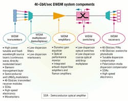
However, the increase in data rates from 10 to 40 Gbits/sec requires upgrades in many components and the introduction of several new technologies. The total cost of these new high-speed links will determine the penetration of 40-Gbit/sec systems into the network.The challenges to the implementation of 40-Gbit/sec systems are significant and require a broad array of specially developed components. Figure 2 illustrates a simplified version of an optical network and notes the components that would enable 40-Gbit/sec systems.
The initial product launches for 40 Gbits/sec will most likely be single-wavelength TDM systems. These initial products will be quickly followed by DWDM systems operating in the C- and L-bands. Initial DWDM channel plans will be 200-GHz spacing, moving toward 100 GHz.
As deployments move forward, it is very likely that the majority of 40-Gbit/sec DWDM sources will be tunable. Tunability will be an important consideration in reducing WDM source laser inventory costs and increasing flexibility. Launch power is important because most WDM systems will be RZ format, which requires an additional modulation stage. Additionally, some TDM systems may use the 1,310-nm spectral window, which has higher absorption than either the C- or L-band.
For fixed-wavelength 40-Gbit/sec systems, there is an effort to develop electro-absorptive modulated lasers (EMLs). These products should offer a lower-cost option for future generations of 40 Gbits/sec. However, it appears that the initial introduction and subsequent WDM systems will be continuous wave sources with broadband external modulators.As with 10-Gbit/sec systems, at 40 Gbits/sec external modulators are used to provide optical pulse generation and data modulation. Current technology for external modulators is x-cut lithium niobate (LiNbO3). However, due to higher drive voltages required at 40 Gbits/sec, there are significant advantages in using z-cut LiNbO3. A number of other materials are under consideration for external modulators using the Mach-Zehnder ap proach, including semiconductors indium phosphide (InP) and gallium arsenide (GaAs) as well as some polymers. It should be noted that these materials have higher losses than LiNbO3, so higher launch power or additional amplification may be required.
Intermediate-reach, short-reach, and very-short-reach applications will most likely use the NRZ format. RZ format will be preferred over NRZ for all long-haul applications. There will also be requirements for up to 7% to 25% overhead in the modulator to allow for forward error correction of the 40-Gbit/sec signal. Other important considerations will be level of integration (co-packaging with the modulator driver and electronic multiplexer), module size, and power consumption. External modulators for 40 Gbits/sec are currently available.
The early generation of the 40-Gbit/sec photodiode will be discrete PIN. How ever, tradeoffs between bandwidth and quantum efficiency of standard surface-normal PIN diodes at 40 Gbits/sec prohibit high responsivity. (Waveguide photodiodes can circumvent this tradeoff, but their edge-illuminated geometry requires micron-scale fiber alignment, and efficient fiber-to-diode mode matching at this level is non-trivial. Innovative schemes can be deployed, such as the use of a refracting facet to create a glancing angle of incidence, which substantially lengthens the optical path through the active region.) Avalanche photodiode technology used at 10 Gbits/sec cannot reach 40 Gbits/sec due to material performance, which limits bandwidth in the presence of reasonable gain.
Discrete analog front-end components (PIN + TIA) will be used at 40 Gbits/sec, but the increased difficulty of interfacing to digital ICs (CDR/demultiplexer) will drive hybrid integration of digital functions with front-end functions into single components. Also, the combination of analog front-end and digital back-end functions into single components will greatly simplify their use by customers. In parallel, the next generation of ICs is being developed in InP, GaAs, and silicon germanium. The more ambitious firms are attempting monolithic integration of PIN and TIA in InP.
It appears that the first analog front-end prototype will be available in the third quarter of this year. The production ramp begins by the end of 2001, and the first integrated receiver with CDR/ demultiplexer prototype will be available by the end of 2001.
Many network equipment manufacturers will require an integrated transmitter/receiver function in the form of a transceiver module. At OC-192, there are a number of firms producing transceiver modules to the Optical Internetworking Forum OIF-5 Multisource Agreement. Creating an equivalent 40-Gbit/sec module will require an even higher degree of electronic component integration.
Serializers and deserializers will need to be combined with optical components such as the modulators and receivers to limit the number of separate coax-connected components. And the next generation of optical receivers will combine optical-to-electrical conversion with clock and data recovery and data demultiplexing. Optical in...digital out.
While OC-768 standards are still evolving, it appears that the most likely format will be a 16:1 and 1:16 approach with input and output line speeds at 2.5 Gbits/sec. The first 40-Gbit/sec transceiver modules are expected later this year, with general availability by mid 2002.
To compensate for dispersion-compensating fiber (DCF) slope errors, network designers have looked toward single-channel tunable dispersion compensators. These devices are used at the receive end of a network span between the receiver demultiplexer and the photodiode.
A number of technologies have been developed for single-channel devices, including fiber Bragg gratings and etalon pairs. Both approaches use differential delays over the spectral pulse to compensate for bulk DCF slope errors. Etalon devices offer many hundreds of psec/nm tuning range and are wavelength independent. Fiber Bragg gratings offer a similar tuning range but are wavelength specific. Both devices are low loss and are typically tuned using temperature effects.
As noted earlier, 40-Gbit/sec systems have a greater sensitivity to OSNR than slower-speed systems. To maximize the span length, all the DWDM channels should be operating at the threshold power level. Consequently, there is a premium on band power uniformity.
An unflattened erbium-doped fiber amplifier (EDFA) can have as much as 6-dB difference in gain (gain tilt) across the C-band. Fixed gain-flattening filters are used to reduce the gain tilt but are limited in their ability to accurately compensate, leading to a ripple of about 0.25 dB. Also, as the gain tilt is a function of the amplifier power, so the ripple will change over time depending on span losses. With five or six EDFAs in a 400-km 40-Gbit/sec link, the accumulated gain ripple could be on the order of 1-2 dB, leading to a reduction in OSNR.
To address the accumulated ripple and modify performance over time, network designers have looked toward a dynamic gain equalizer. Several companies offer this type of device. In principle, these devices operate as a series of single-channel variable optical attenuators integrating the multiplexing and demultiplexing functions over the band of interest. These devices are typically produced using a dispersive demultiplexer illuminating a series of liquid-crystal attenuators, followed by a multiplexer back into the fiber.
Newer generations of dynamic gain equalizers may use micro-electromechanical systems-based attenuators. These devices may also include an integrated optical performance monitor to measure the amplifier performance and the post-amplification gain tilt. Desirable performance parameters include broad spectral range, high slope capability, minimum ripple, low insertion loss, and fast response time.
For 40-Gbit/sec systems, Raman amplifiers offer several advantages over EDFAs. Due to the nature of distributed amplification, they offer reduced noise figure penalty. Adjusting the power levels of multiple pump lasers can control gain flatness to best match the requirements for a given system configuration. The overall performance of the Raman amplifier is dictated by the choice of pump laser wavelengths, power levels, and the use of the appropriate type of transmission fiber.
Hybrid (EDFA and Raman) amplification has been used in a number of 40-Gbit/sec designs to obtain the necessary OSNR. In the EDFA/Raman combination, the Raman pump propagates in the backward direction to boost the signal toward the end of the span lengths. This backward amplification occurs when the OSNR is most likely to deteriorate to unacceptable levels.
Raman amplifiers for 40 Gbits/sec are currently available. Using Raman amplification in this case is similar to a pre-amplification stage in complex EDFAs and results in effectively increasing the distance between optical repeaters. It also provides additional margin in system design.
Compensating for PMD in an optical transmission system is particularly challenging. Unlike chromatic dispersion, which is relatively stable with time, PMD can change significantly over time and requires active control. Accordingly, a PMD compensator requires degree of polarization (DOP) measurement to provide the closed-loop feedback. DOP sensors are typically made from birefringent crystals, which are used to establish the phase delay for the polarization states. Vendors offer DOP monitors that allow PMD measurements from 0.1 to 80 psec.
PMD compensators can be produced by several approaches, including a highly birefringent material such as LiNbO3, a bulk phase retardation plate, or polarization-maintaining fiber. Tunable PMD compensators are new products in the market and should be generally available during the second half of this year.
Much of the focus of this article has been on active components for 40-Gbit/sec links. However, there are a number of passive components that can also influence the performance of 40-Gbit/sec signals. These components include interleavers, DWDM filters, splitters, and combiners. Bulk optical devices, thin-film filters, and fiber Bragg gratings currently used for multiplexing and demultiplexing applications may exhibit modest amounts of dispersion. Care should be taken when specifying these products. Theory indicates that array waveguide grating devices do not contribute to system dispersion.
- "Optical Networks: A Practical Perspec tive", Rajiv Ramaswami, Kumar N. Sivarajan, Morgan Kaufmann Publishers, San Francisco, 1998.
- "Raman Amplifications Design in Wavelength Division Multiplexing Systems Tutorial," Virtual Photonics Inc., http.//www.iec.org/tutorials/raman/ topic03.html.
- "High-speed Optical Transmission Systems," Hiroshi Hamano, et. al., Fujitsu Sci. Tech. J., 35, 1, July 1999.
John Fritschen is manager of business development, optical research, and Stan Lumish is vice president of optical research at JDS Uniphase (Santa Rosa, CA). They can be reached at [email protected]and [email protected] uniphase. com, respectively.


