Amplification advances show promise for all-optical networks
New levels of monolithic integration in planar waveguides and low-cost pumps spawn a new category of amplification devices.
DR. JOYCE KILMER, Symmorphix Inc.
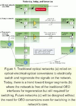
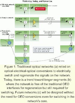
The practical deployment of an all-optical network is probably still a few generations away. But a clear trend is already emerging toward ever-longer segments of optical-network transparency, where the network infrastructure remains free of the traditional optical-electrical-optical (OEO) interfaces used to electrically switch and regenerate the signals on the network (see Figure 1).
This ongoing progression from an electrical to an optical switch fabric promises to dramatically cut network costs, reduce equipment footprint requirements, and improve designer flexibility. The OEO conversion equipment that traditional networks rely on is both expensive and bulky. Eliminating these devices will not only save cost and space, it will enable networks to more easily support a wide variety of services using any number of protocols.
To reach this goal, component developers will have to overcome some significant challenges, however. The OEO conversions play a crucial role in network nodes. The signal conversions allow the system designer to compensate for node loss and dynamic network behavior, which requires channel balancing. The overriding question for network designers is how to extend the reach of an optically transparent network and still provide the functionality supplied today by the OEO conversions.A number of options are available. Fiber amplifiers such as erbium-doped fiber amplifiers (EDFAs) or Raman amplifier modules employ high-power pump source lasers to provide the high gain and power needed to simultaneously boost a full C-band of DWDM wavelengths. Often deployed in series to overcome span losses, fiber amplifiers can significantly extend the reach of long-haul systems.
For node losses, a new generation of amplets, enabled by recent advances in monolithic integration in planar waveguides and low-cost pumps, offer a more attractive option. Deployed in parallel arrays to support per-channel amplification or channel balancing, these low-power devices feature modest gain and are used to boost individual wavelengths or "color bands." Amplets generally offer a significantly lower cost than full-band fiber amplifiers by using lower-cost, lower-power pump sources. These devices also tend to be significantly more compact than their full-band cousins.
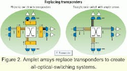
With the introduction of monolithic integration in planar waveguides and low-cost pumps, amplets are increasingly used in a wide variety of applications to extend the reach of optically transparent networks. One example is optical crossconnects (OXCs). The current generation of these devices typically features an optical switching fabric such as an NxN micro-electromechanical-systems (MEMS)-based matrix switch. The optical switch is often surrounded by devices known as transponders, which perform a form of OEO conversion. The transponders detect a 1,550-nm DWDM signal and convert it to an electrical signal to drive a standard 1,310-nm short-reach SONET transmitter. This 1,310-nm signal is switched through the optical-switching fabric and detected by the destination transponder, which in turn converts it back to the 1,550-nm ITU grid wavelength. In some cases, equipment designers must move from less expensive, lower powered short-reach SONET transmitters to more expensive, medium-reach transmitters because the optical-switching fabric is so lossy, the short-reach devices do not have sufficient power. In these cases, arrays of amplets can be used to inexpensively increase the output power of the short-reach SONET transmitters.
The next generation of OXCs, according to development plans, will eliminate these costly OEO transponder wraparounds and switch directly in the C-band. A variety of optical-switching-fabric technologies is available with differing cost and loss versus scaling tradeoffs. But designers may find it is more cost-effective to use a less expensive switching technology in concert with arrays of amplets (see Figure 2).Another potential application for amplets is in the migration to scalable switch technologies. Since it may not be cost-effective to immediately deploy an OXC with an extremely high port count, many carriers may opt to use multiple optical-switching fabrics with lower port counts as building blocks to scale their networks. In such a configuration, loss will scale with the number of ports. An amplet array, used in an incremental manner, can help to address those losses.
As network designers scale from 10-Gbit/sec OC-192 to 40-Gbit/sec OC-768 systems, they will confront a greater need to control the optical fibers' natural impairments. In many cases, network operators deploy dispersion compensators and polarization controllers to address this need. Since these devices also contribute to node losses, amplet arrays may be used to address these losses, as well.
The tunable-laser source is another component likely to emerge in future-generation networks that may benefit from the use of amplets. Tunable lasers often sacrifice output power to achieve wavelength tunability. In some cases, their power is so low that the tunable laser cannot be used with an external modulator. In these instances, compact amplets may help make these sources usable.
While conventional EDFAs are typically deployed with the static optical add/drop multiplexers (OADMs) used today, space and flexibility constraints may make it difficult to use these amplifers with future devices that offer dynamic reconfigurability.
Static and dynamic OADMs use similar architectures. In both types, a demultiplexing device splits an incoming DWDM signal stream into its constituent wavelengths. An array of 2x2 switches dictates which wavelengths are passed through the node or dropped. If a wavelength is dropped, a new signal can be placed on that wavelength and added back into the system. An array of electrically controlled, variable optical attenuators (VOAs) balances the power of individual wavelength channels. Each channel is then multiplexed out of the node. This power balancing prevents a line EDFA from preferentially amplifying one wavelength at the expense of another.
The basic difference between a static OADM and dynamic OADM is remote control of the switch and VOA arrays. A major reason why network designers want to move to dynamic OADMs is that a technician must be dispatched to the remote node to manually reconfigure a static OADM.
Unfortunately, since arrays of electrically controlled switches and VOAs are typically constructed from discrete devices, they significantly increase the size of reconfigurable OADMs. Moreover, the ongoing trend to higher DWDM channel counts within the C-band is pushing the capabilities of thin-film-filter and fiber Bragg grating-based DWDM designs. New technologies such as arrayed-waveguide-grating (AWG)-based multiplexing and demultiplexing devices offer a better solution. But devices based on these technologies often contribute 6-dB excess loss for both the multiplexing and demultiplexing functions. In addition, the natural excess loss of a 2x2 switch and VOA can add another 1 or 2 dB. Consequently, some sort of amplification is essential to counteract a node loss in the OADM that could reach 14 to 16 dB.
In these applications, amplets not only provide the required gain, but these devices also give designers the opportunity to eliminate the VOA. While it is designed to bring the highest-power signal level down to the lowest-common-denominator signal level, a VOA also wastes optical power and affects the signal-to-noise ratio. A more attractive solution is the use of amplet arrays with variable optical amplification. These devices are designed to bring weaker signals up to the level of the strongest signal and in the process simplify signal-to-noise management and overall system design.
Finally, a growing interest in passive-optical-network (PON) architectures using either ATM or Gigabit Ethernet signaling has created another potential application for amplets in the access market. Promoted as a cost-effective way to bring deployment of fiber closer to the home, PON-based architectures use 1xN splitters in the outside plant to enable a single fiber from the central office to be shared among multiple users in the access loop. The use of amplets can help compensate for the loss generated by these 1xN splitters.
Today, several technologies are emerging to meet the rapidly growing need for amplification distribution. The EDFA was one of the first products to reflect the ongoing evolution of photonics to hybridized modules from discrete components. It consists of a number of discrete components that are fusion-spliced together. The EDFA is built around a WDM coupler or pump combiner that mixes the pump-laser wavelength (980 nm or 1,480 nm) with the signal wavelengths (usually in the 1,530-nm to 1,565-nm range). The output fiber of the pump combiner is fusion-spliced with some erbium-doped fiber in a process, which, due to the material differences between the two fiber types, often results in a very fragile splice. To protect the splice, designers place a heat-sink protector over it. Finally, one or more optical isolators are often spliced into the optical path to ensure proper performance from the EDFA and prevent unwanted reflected or backscattered light from traveling upstream.
Altogether, a simple single-stage EDFA can combine more then 10 discrete components. Moreover, all slack fiber between components must be controlled and coiled to no less than a 1-inch bend radius to prevent macrobending-induced loss at the longer wavelengths. Such complex production requirements typically require extensive manual labor by highly skilled technicians and do not lend themselves to cost-effective, high-volume manufacturing.
Raman amplification is another alternative. This natural, nonlinear phenomenon is evoked by launching high total optical power levels into a fiber. Recently, it was successfully used to distribute amplification along the length of a fiber. Raman amplification technology offers unique attributes. Since the signal is amplified continuously along the fiber's length, some portion of the signal is actually amplified before it becomes noisy. In this way, Raman amplification can actually achieve a negative noise figure. However, due to its distributed nature, Raman amplification requires a long fiber length to be effective. Accordingly, it cannot be used to compensate for loss in the short distances found within nodes.
One of the first attempts to build amplifying optical components was centered on the semiconductor laser diode. Designers tried to bias the structure enough electrically so that it was just below its oscillation threshold, then used an antireflective coating on the facets of the device to prevent lasing. That allowed a weak optical signal coupled into the rear facet of the device to exit the front of device in an amplified state. Unfortunately, this type of gain process is inherently noisy and subject to polarization problems. It is difficult to manufacture semiconductor optical amplifiers with less than a 10-dB noise figure (NF). Furthermore, low process yields make it extremely difficult to produce these devices cost-effectively.
The most commonly used solution in commercially deployed DWDM optical-fiber systems today is EDFAs. In recent years, manufacturers have learned how to produce these devices with gains as high as 30 dB and NFs around 5 dB over the full 1,530- to 1,565-nm C-band spectrum. However, these modules integrate a large number of discrete components in a complex manufacturing process.
An alternative approach is based on early work in planar optical-waveguide amplifiers demonstrated by a team at Bell Labs. This technology dopes the same erbium ions used in an EDFA into a planar waveguide on a chip. These so-called erbium-doped waveguide amplifiers (EDWAs) produce about 4-dB gain per centimeter in an EDWA with a relatively low 5-dB NF.
But developers of these devices face significant challenges. To achieve low losses and NFs, EDWAs must have high-quality fiber-to-waveguide coupling. Yet, unlike fiber amplifiers, these devices cannot rely on fusion splicing of fibers. In addition, waveguide materials are generally not as transparent as fiber, so absorption and scattering losses must be lowered. Finally, the rare earth dopant composition must be optimized for high gain in a short length without high upconversion losses. Since EDWAs may use similar fabrication processes to other planar integrated component devices such as splitters and AWGs, they are highly manufacturable. If these design challenges can be overcome, EDWAs will present a very viable solution for compact point amplification.
As demand grows for a wide variety of broadband services, pressure is mounting on carriers to build all-optical networks capable of delivering those services. One of the most formidable obstacles network developers face in that task is the elimination of the OEO interfaces deployed throughout today's networks. These conversion systems currently constitute up to half of the cost of building and operating an optical network.
To eliminate those costly interfaces, network designers will need new technologies capable of optical amplification everywhere to overcome signal loss. At the same time, optical networks will require increasingly compact components capable of packing higher levels of functionality into existing racks and closets, particularly as networks expand to support greater capacity and performance.
Clearly, the key to solving this problem is the development of a new generation of optical components, which bring new levels of integration. These components must offer a highly flexible architecture capable of amplifying a single wavelength, sub-band, or full band, as optical channels migrate from whole fibers to individual wavelengths. Scalar planar integrated devices offer the most promising solution to this problem.
Dr. Joyce Kilmer is manager of field application engineering at Symmorphix Inc. (Sunnyvale, CA). Dr. Kilmer can be reached by e-mail: [email protected].


