Advances in packaging automation critical to reducing costs
For laser diodes to power the optical network, automated packaging is paramount to component manufacturers.
Photo courtesy of Advanced Packaging
BRUCE HUENERS, Palomar Technologies
Laser diodes power the optical network. As source lasers, they convert high-frequency electrical signals into high-data-rate optical pulses to send down optical fibers. As pump lasers, they amplify the source laser signal to extend its reach in long-haul and metro optical transmission networks. In only two decades, the semiconductor laser diode has evolved into a family of robust, reliable devices with individual conversion efficiencies of better than 50%, continuous output powers of several kilowatts, modulation rates of several tens of gigahertz, and wavelengths from 450 nm to beyond 2000 nm.
The presence of the laser diode in the optical network is ubiquitous and growing. Current forecasts predict a 35-45% compound growth rate in just the edge-emitting segment of this market.
Additionally, the package containing the laser diode accounts for an estimated 60-80% of the current manufacturing expenses in optoelectronic assembly. Consequently, advances in packaging automation are critical to reducing costs in the optical network. Established component manufacturers have quickly discovered that simply increasing their manual workforce will not meet the demand. Startups have realized that a manual assembly process cannot be used to meet the time-to-volume requirements necessary for them to rapidly establish market share.Automation provides the following benefits to laser-diode production:
- Yield improvements (through reduction of scrap and rework).
- Throughput increases (raw output).
- Productivity increases (output per square meter of factory floor space).
- Reduced time to scalable volume manufacturing (accelerating capture of market share).
The optoelectronic-component industry is currently capacity-constrained and labor-intensive, with predominantly piece-part assembly that is not scalable. Consequently, component manufacturers, both large and small, are investing in automation to reduce cost, increase yield, and gain productivity.
Proprietary methods and high intellectual property barriers are prevalent in the industry today. These methods include custom wafer processing, thin-film processing, device and subassembly packaging (including eutectic and epoxy component attach and wire bonding), fiber handling and alignment, and the finish steps of tuning, adjusting, and testing. Furthermore, multiple fabrication techniques and processes are common, coupled with a lack of package and material handling standards.Industrial engineering approaches common in other technology industries are largely absent from today's photonics manufacturing environment. These practices include process engineering, design for manufacturing, design for test, standardization, outsourcing, and automation. They are highly interrelated, and any discussion of automation must include these practices together with the specific types of materials employed in optoelectronic components.
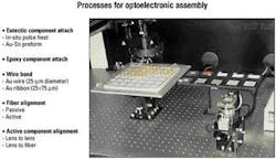
Since the optoelectronic package is a hybrid processor of both electronic and photonic signals, there are a plethora of unique materials used in device fabrication. This variety of materials is one of the factors that distinguishes optoelectronic device assembly from conventional microelectronic assembly. The Table lists some of the materials used in optoelectronic-device fabrication.Processes for optoelectronic assembly today include many traditional microelectronic assembly processes and a few special processes with the added complication of fiber alignment and active-component alignment (see Figure 1). During the device fabrication process, external stress may be applied to the diodes. In the cleaving of the processed wafers into diode arrays, mechanical damage can be induced from the cleaved edge of the crystal. In some cases, dislocations are generated from such regions. During die attach or wire bonding, thermal or mechanical stress is applied to the diode chips, which may accumulate elastic strain in the diode or generate mechanical damage or scratches in the crystal. To minimize stress, this assembly process should be automated and recipe-driven for extremely repeatable and consistent results.
Implementing a high-yield, fully automatic assembly process for optoelectronic packaging requires specialized ma chine functions. This machine functionality may be grouped into three categories: precision motion, machine vision, and recipe-driven process control.
Precision motion. Precision motion is required in multiple axes. For example, precise motion control is required for force application, while the position of each machine axis must be dynamically monitored. Precision force control is necessary for many reasons:
- It is critical for consistent handling of fragile devices such as indium phosphide (InP) and gallium arsenide (GaAs).
- Programmable descent velocity and acceleration profiles are needed to pick and place these devices.
- A low force touch and programmable ascent profile is required to pick fragile devices from presentation formats such as waffle pack, gel pack, tape and reel, and expanded wafer.
Dynamic z-axis monitoring is a prerequisite to automating optoelectronic assembly. That includes position monitoring for consistent spatial placement, real-time closed-loop monitoring, and histograms created from final recorded position. Users can specify a process range of acceptable z-position.
Machine vision. For fully automatic operation, machine vision is required for part recognition, alignment, and positional verification. High-resolution machine vision enables accurate bond placement, 0.1 pixel resolution, 256 levels of gray scale, and pre- and post-bond inspection.
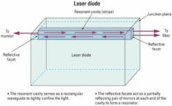
Recipe-driven process control. The importance of recipe-driven process control for optoelectronic assembly may be illustrated by considering the case of attaching a laser diode within a source or pump laser. As Figure 2 shows, the active device in source and pump lasers is commonly an edge-emitting semiconductor laser diode. That is an extremely temperature-sensitive device requiring careful process control during assembly.In a diode laser, the amplifying element is a forward-biased PN junction formed in a direct bandgap semiconductor. Optical gain is provided by the recombination of electrons and holes in the PN junction. When forward-biased above the bandgap energy, electrons are injected from the N side while holes are injected from the P side, forming a "population inversion" near the junction-a necessary state for lasing to occur.
Electrons and holes are confined within a lower bandgap region where they can recombine either spontaneously or via stimulated emission when excited by an existing photon. The resonator continuously recirculates light and amplifies through stimulated emission. The resonator is responsible for the high level of coherence in a laser, both spatial (focusable to a very small spot) and spectral (consisting of a narrow range of frequencies). In a laser diode, a waveguide confines the light in two dimensions, causing it to travel back and forth along a predominantly linear path.
The output of a laser diode depends on the drive current passing through it (as long as the bias voltage is above the bandgap energy). The operating temperature of the laser is a key factor in device reliability, as threshold current tends to increase with temperature, thus increasing the amount of waste heat generated. Furthermore, laser lifetime decreases as temperature increases.
Given the foregoing device requirements, it is clearly evident how recipe-driven process control is essential in the fabrication of laser diodes. To optimize heat transfer, laser diodes are attached via a low-ohmic, high-thermal conductivity metalization in a precisely controlled environment through a eutectic reflow process.
Consider the case of Raman amplifiers, where higher optical power levels are being achieved at 1400 to 1480 nm. This higher power, combined with lower manufacturing costs, has resulted in a major increase in the demand for 1480-nm pump lasers. For Raman amplifiers, increasing output levels is necessary to provide the needed gain margin for DWDM applications as well as additional flexibility for amplifier designers.
One of the benefits of higher laser-chip power in Raman amplifiers is improved power linearity in modules. In the 14xx module, thermal effects significantly limit the fiber power linearity, leading to a condition called thermal rollover, which occurs when increases in operating current no longer produce additional output power. This rollover condition occurs independent of laser mode and waveguide losses and is strictly associated with the overall thermal properties of the laser chip and package. Thus, thermal rollover can occur while the singlemode behavior of the chip remains unchanged.Although thermal saturation does not alter chip-mode stability, it does significantly impact power linearity. In other words, slope efficiency is reduced with increasing output power. Thermal rollover effects observed 50 to 100 mW above the recommended module performance level may lead to reduced performance between beginning-of-life (BOL) and end-of-life (EOL) module characteristics. The module performance change between BOL and EOL is about 10-20%.
The case of Raman amplifiers emphasizes the need for automated, recipe-driven process control for efficient production of these devices. Precision eutectic component attach includes:
- Pick and place of silicon (Si), GaAs, or InP chips.
- In-situ reflow of preform or pre-tinned devices, in concert with programmable x-, y-, or z-axis agitation.
- Programmable pulse heating or steady-state temperature.
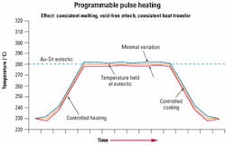
The reflow profile during an in-situ eutectic die attach process is engineered to provide consistent melting and a void-free attach interface (see Figure 3). That results in consistent heat transfer from the laser diode and contributes significantly to temperature stabilization during laser operation.
Programmable pulse heating, coupled with automated component attach, provides the recipe-driven process control essential to producing high-yield, high-performance laser-diode assemblies. During the in-situ reflow process, temperature slopes for heating and cooling, overshoot, and dwell times are programmable to enable process optimization and repeatability. Tightly coupled temperature control ensures profiles are tracked repeatedly in production.With tangible benefits capable of being realized today, optoelectronic manufacturers are pulling automation into their factories. However, they are facing considerable challenges. Some factors affecting photonic package assembly strategy include accelerating the use of automation in fiber-optic-component manufacturing, which will require:
- Accommodating complex proprietary methods in automated equipment.
- Finding commonalities in multiple fabrication techniques and processes.
- Designing components for automation.
- Establishing package- and material-handling standards.
The first true automation in the in dustry for first-level interconnect came from adapting existing automated die attach and wire bonding equipment to meet the needs of optoelectronic-component manufacturers. The industry has found the wire bonding and die bonding equipment that was designed over the past decade for the high-performance hybrid, multichip module, and microwave industry can be used as off-the-shelf solutions for automating certain processes in the optical industry.
Three important competencies are required for an automation supplier to effectively provide solutions to the optoelectronic-device manufacturer: the "toolset," "experience base," and "process engineering skillset."
The toolset is the range of equipment specifically tailored to perform optical-component assembly. This equipment is capable of performing precision alignment and interconnection of components and includes die bonders, wire bonders, and alignment stations, together with the capability for joining these functions together in an integrated solution (see Figure 4).
Equally important is the experience base and process engineering skillset specific to optoelectronic automation. The experience base is the relevant background developed in associated assembly applications, notably the applications that most closely parallel optoelectronic assembly. Associated assembly applications, including those in the disk-drive, aerospace and defense electronics, semiconductor, automotive, and medical industries all serve as an extremely relevant precursor to the requisite capabilities for optoelectronics assembly.
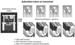
The process engineering skillset is the array of competencies for implementing the toolset and drawing on the ex perience base to provide a total solution. These competencies include skills in die bonding, wire bonding, and process integration.Automation can bring significant cost savings to the optoelectronic assembly industry. A component manufacturer demonstrated that one automated eutectic die attach machine could produce the same total output as four manual stations run by 20 operators. Further more, when using the automated process, yielded output went up by 50%, with a 67% reduction in occupied floor space in the cleanroom (see Figure 5). These savings resulted in the realization of return on investment on the equipment in less than three months.
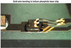
Manufacturers have also incorporated automatic wire bonding stations in their manufacturing processes to deliver repeatable first-level interconnects significantly faster than with manual stations. Deep-access wire bonding is another process easily adopted into the optoelectronic-component manufacturing industry based on years of previous development in the high-frequency wireless and hybrid semiconductor markets (see Figure 6).
With bit rates projected to reach 40 Gbits/sec and higher this year, predictable and repeatable wire and ribbon bond lengths, loop profiles, and tail lengths will be an essential part of component design and packaging. These critical parameters are nearly impossible to achieve manually and will necessitate the proliferation of automated solutions throughout the industry.
Converting an industry from a largely manual assembly process to an automatic assembly process requires close partnership between automated equipment suppliers and device manufacturers. The automation can be viewed as a three-phase process:
- Phase 1, manual and semi-automatic processes.
- Phase 2, islands of automation implementing individual processes.
- Phase 3, integrated lines linking multiple processes in a continuous flow.
Any device manufacturer seriously considering automating its optoelectronic assembly operation should consider the following factors that affect automation strategy:
- Product volume
- Expected product lifecycle
- Design changes in the product
- Handling requirements
- Product mix (number of different types of products)
- Product complexity
- Degree of required operator skill
- Cost of labor
The first phase of automation normally focuses on a specific process that uses equipment to perform the precise assembly operation (such as laser-diode attach) and employs an operator to batch load the machine. That enables the device manufacturer to concentrate on critical processes that provide the highest payback from automation.
The second phase further mechanizes the island of automation by implementing automatic load and unload of material. That can be especially effective in optoelectronic assembly as it further removes the influence of the operator in the process (resulting in increased yield).
The third phase, coupling several automated processes in an integrated production line, is the highest form of automation. This implementation can permit the highest assembly yield due to short feedback loops) and highest volume with lowest assembly cost.
Currently, the optoelectronic-component manufacturing industry is capacity-constrained and facing a projected annual growth rate in demand of 35-45%. Most manufacturers have recognized that a paradigm shift in assembly methods will have to take place for them to meet demand. That shift is emerging as a move from the manual assembly processes that have characterized the industry for decades to high-accuracy, high-throughput automated manufacturing.
Device manufacturers should evaluate potential automation suppliers ac cording to the following checklist:
- Ability to supply a total solution, including hardware, process, and support.
- Photonics automation experience with relevant hardware and process expertise.
- Ability to partner with the manufacturer and the flexibility to customize solutions, including helping to design products for automation.
While automation will eventually provide complete process solutions for the optical-component assembly industry, there are significant challenges to automation. The combination of extreme accuracy requirements, significant variations in height, unusual form factors, unusual materials, and the inherent difficulties arising from the requirement to guide light have prevented most equipment available today from being used for optical-component packaging.
Fortunately, there are a few systems available that have the flexibility to support these difficult tolerances. Specifically, die attachment and wire bonding techniques that were developed in the hybrid semiconductor and high-frequency wireless industries are currently being incorporated in the optical-component manufacturing industry. The early results from the implementation of this equipment are encouraging. Companies have experienced an in crease in yielded throughput and a reduction in required cleanroom floor space by replacing several manual die bonding stations with a single automatic die bonder. Furthermore, automated wire bonders are facilitating the move to higher-frequency devices, since they have superior control of wire length and loop profiles when compared to manual processes.
We are now seeing the emergence of an equipment-supplier base that can support the stringent tolerances of the optoelectronic-component assembly industry. The equipment these suppliers are designing today will not only facilitate the efficient manufacture of optical components, but also will enable the component designers to continue to push the envelope of communications technology into the foreseeable future-where laser diodes will continue to power the optical network while automation powers their efficient production.
Bruce Hueners is director of marketing at Palomar Technologies (Vista, CA). He can be reached at www.bonders.com.
- Morgan Stanley Dean Witter.
- National Institutes of Standards and Technology.
- O. Ueda, Reliability and degradation of III-V optical devices, Artech House, 1996.
- R. Lang, "Semiconductor lasers: an overview of commercial devices," Photonics Handbook, Book 3, p. H-227, 2001.
- J. Connolly, WDM Solutions, 57 (June 2001).


