MEMS helps measure high-density wavelengths
With the increase in wavelength density and bit rates in WDM optical communications networks, quality of service (QoS) has become a critical issue. Conventional test instrumentation does not have the scan rate or a wide enough scan wavelength range to perform the necessary high-speed dynamic spectrum monitoring required for fiber-Bragg-grating (FBG) sensors and photonic networks. However, a new generation of test instruments that utilizes MEMS technology is providing the performance as well as reduced cost and size necessary for these high-bit-rate applications.
MEMS technology offers significant advantages over conventional technology used in test instrumentation. MEMS can be integrated into instruments such as optical spectrum analyzers (OSAs) and WDM optical monitors to measure high-speed optical phenomena that cannot be accurately observed by traditional instruments.
That is a natural progression of technology, since MEMS is part of many of today's optical equipment designs. The reason is simple: MEMS has a number of inherent advantages over older technologies. It integrates mechanical elements, sensors, actuators, and electronics on a common silicon substrate. The electronics are fabricated using IC process sequences like complementary metal-oxide semiconductor (CMOS), bipolar, or bipolar CMOS, while the micromechanical components are fabricated using compatible "micromachining" processes that selectively etch away parts of the silicon wafer or add new structural layers to form the mechanical and electromechanical devices.
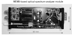
Microelectronic ICs are typically referred to as the "brains" of a system. MEMS augments this decision-making capability with "eyes" and "arms" so microsystems can sense and control the environment. Sensors gather information by measuring mechanical, thermal, biological, chemical, optical, and magnetic phenomena. The data acquired by the sensors is processed by the electronics, which based on this data instructs the actuators to respond in a specific manner. In short, MEMS devices allow extremely high levels of functionality, reliability, and sophistication to be placed on a small silicon chip at a relatively low cost.MEMS technology can be employed in an OSA to measure WDM signals more accurately. An OSA module consists of lenses, Faraday rotator, diffraction grating, MEMS optical scanner, and one photodiode (see Figure 1). Light from the fiber is input to the module and, after being collimated by a lens, impinges on the diffraction grating. The diffracted light strikes the MEMS optical scanner and is reflected back to the diffraction grating. Finally, the diffraction grating sends specific light to the photodiode. The light sent to the photodiode can be changed continuously by rotating the MEMS scanner.
The Faraday rotator is incorporated into the module to erase polarization dependency of the diffraction grating if an unknown polarized input has to be measured. The module driver generates a signal for the MEMS optical scanner. The photodiode's output signal is converted to a digital signal using an analog-to-digital converter. That allows the input light's spectrum to be digitized so the measurement results can be displayed on a PC.
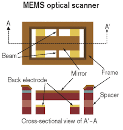
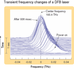
Figure 2 shows the MEMS optical scanner. It consists of a mirror, two beams, a frame, spacer, and back electrodes. Silicon deep reactive ion etching and potassium hydroxide (KOH) anisotropic chemical etching are used for the fabrication process. The mirror, spacer, and back electrodes are fabricated separately from silicon wafers and glued together to form the final scanner shape.The benefits of using MEMS in an OSA module are evident when measuring two spectra changing at high speed. One measurement is the observation of transient frequency changes of a DFB laser with a 10-mW output and 193.4-THz frequency. The laser is equipped with an automatic power control circuit and automatic temperature control circuit. Figure 3 shows the measurement results of transient frequency changes of the output from the DFB laser after power-on at 26-msec measurement intervals. Stabilization clearly takes 936 msec. Obvious changes in both the frequency and output level can be seen.
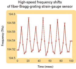
Improved measurements on FBG strain-gauge sensors can also be realized. Strain on the sensor is measured by observing a center frequency shift acquired by using a wideband optical source and spectrum analyzer. The results of applying a frequently changing force of 75 Hz to the sensor are shown in Figure 4. Measurement results of center frequency shift of the sensor during 100 msec are also shown. High-speed frequency shifts such as that are difficult to measure using a conventional OSA.As with OSAs, the use of a MEMS optical scanner in WDM monitors can improve measurement accuracy of WDM signals. Presently, the WDM optical monitor is the test instrument of choice for assuring the performance of WDM networks. These WDM optical monitors are developed using one of two designs, neither of which provides the cost/performance ratio necessary for field use. One design uses a large number of small photodiodes to cover a broad bandwidth with sufficient resolution. The second design uses a MEMS-tunable Fabry-Perot filter consisting of a stable mirror and moving mirror. While it employs a degree of MEMS technology, the design is not effective because it does not move the one mirror fast enough.
A MEMS-based WDM monitor module consisting of a collimator, Faraday rotator, grating, silicon MEMS optical scanner, etalon, and photodiodes is now under development. With this module, WDM optical monitors will have the performance and price point necessary for ensuring the performance of WDM networks.
The module incorporates a straightforward measuring technique. The input light is collimated by the lens, passes through the Faraday rotator, and impinges on the grating where the light is diffracted. The first-order diffracted light strikes the mirror of the MEMS optical scanner and is reflected back toward the grating where it is diffracted a second time to form a Littman-type optical filter.
There are a number of similarities between this WDM module and the one for OSAs. First, the MEMS optical scanner is actuated electrostatically by mechanical resonance. Second, the input light's wavelength changes continuously and cyclically based on the rotation angle of the MEMS scanner, which can be set by the user. Also, the Faraday rotator is used to erase polarization dependency of the grating. Unlike the OSA module, the WDM monitor module has an etalon to compensate the measurement result.
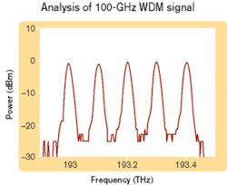
By measuring the output voltage of the photodiode and using the rotation angle of the MEMS scanner, it is possible to measure the spectrum of the input WDM signal. An example of the accuracy achieved by using the MEMS-based technique to measure a 100-GHz-spaced WDM signal is shown in Figure 5. The measurement speed is 5.2 msec, including calculation by the PC, and the resolution is 0.16 nm. The optical spacing is detected with much more precision than if a conventional photodiode array were used.In addition to increasing performance so test solutions can meet requirements created by higher bit rates, MEMS technology can aid in the size and cost of instruments. The size reduction can be fairly dramatic since the WDM module using a MEMS optical scanner measures just 90×40×20 mm. It also promises lower cost because the MEMS technology eliminates the need for multiple photodiodes.
Since there are many field applications for these instruments, smaller size and lower cost can be quite advantageous. Field technicians can conduct QoS measurements without carrying bigger, heavier instruments, allowing technicians to be more efficient. Additionally, the price savings will reduce the cost of maintenance and allow carriers to reap better profits.
Wavelength density and bit rates will continue to increase with each new generation of optical communications networks. Conventional test instruments using older mature technology do not have the capability to accurately and affordably measure these higher bandwidths.
MEMS technology provides a viable solution to these testing requirements. OSAs and WDM monitors that utilize MEMS-based modules can measure high-speed optical communications networks with the necessary speed and accuracy. The utilization of MEMS technology also results in smaller, more cost-effective test solutions—two vital factors when considering instruments for field use.
Takanori Saitoh is an expert research engineer at Anritsu (Kanagawa, Japan). He can be reached at +81-46-296-6542 or [email protected].
