Optical switching: More choice, more efficiency
Among the many all-optical choices today, one technology is emerging that demonstrates practicality and flexibility.
TOM ALBERTSON, Agere Systems
The astounding progress in fiber-optic technologies has created information networks whose capacities and capabilities were unimaginable less than 20 years ago. Technological progress has also created intense marketplace competition, raising the bar for survival and success. In today's competitive economic environment, service providers must manage their optical-networking assets with maximum efficiency and economy, carefully balancing current needs to reduce operating expenses against the requirement to provide forward-looking network infrastructures capable of meeting future demands.
Network managers increasingly are betting on all-optical networking for their fiber-optic infrastructures. The development of protocol-independent, rate-independent switching fabrics that avoid the complexity and performance problems associated with today's largely optical-electrical-optical (OEO) devices-and provide current operating benefits along with the scalability to meet future demands-will largely determine the outcome of this wager.
While several all-optical techniques are available now, the emerging choice for forward-looking switching arrays is three-dimensional micro-electromechanical systems (3-D MEMS). This technology is not only the sole practical approach for large-scale switching arrays, but is also scalable to larger and smaller arrays as well.
3-D MEMS provide the immediate benefits of protocol and rate independence, low overall signal loss, small form factor (SFF), and competitive switching speeds. 3-D MEMS also have the potential for vast improvements in all performance parameters. In addition, the silicon-based fabrication techniques used in making 3-D MEMS promise ever-higher levels of integration of control and management electronics on MEMS arrays, which can greatly enhance network-management capabilities and operating efficiencies.
The ever-more-capable communications and information systems resulting from fiber optics have raised users' expectations. Despite the current "glut" of fiber in the ground, there has never been any serious question about the need for additional bandwidth. In every era, with every new technological breakthrough, carriers and their customers have called for more.
But capacity is only one dimension of the challenge carriers face in satisfying users' needs. They need to manage their current assets to maximum advantage and lay the technological groundwork for future systems and services. That is especially critical in an era where DWDM systems are becoming ubiquitous. Now network providers have the challenge-and opportunity-to manage wavelengths instead of fibers, enabling them to build networks that speed the introduction of new services while vastly enhancing operational efficiency and economy.Fiber-optic networks must deal with a variety of service and transport protocols and speeds as well as dynamic service and configuration demands. Carriers must operate optical networks that provide transport flexibility, are independent of bit rate and format, and permit efficient rearrangement of embedded capacity as demand patterns change.
Optical networks must provide reliable optical-channel routing and transport for the service layers (IP, TDM, ATM) they support. To do so, optical networks must include bit-rate-independent, protocol-transparent photonic switches and crossconnects. That is a tall order, taxing systems designers to balance the need for short-term results with long-term competitive advantage.
The compound annual growth rate of optical-crossconnect-system sales has been forecast by KMI Corp. (Providence) to rise 124% through 2006 while per-port prices are forecast to decline 31% per year. KMI estimates that the market rose from $50 million in 2000 to more than $400 million in 2001 and will reach $6.3 billion by 2006, due to higher-port-count products, penetration into smaller offices, and expanding regional sales. KMI also predicts that optical crossconnects will be the choice for the future, saving up to 70% of network costs when compared to SONET equipment and allowing more speed and capacity per unit.
Currently, network designers and systems engineers have three basic technological choices for all-optical-switching fabrics: bubble, liquid crystal, and MEMS.
The first of these approaches is based on the technology used in bubble jet printers. The device has a dual-layered architecture: a top layer of silicon that holds the ink-pen technology used in bubble jet printers and a glass layer on top through which multiple light signals travel. The bottom layer has 32 parallel waveguides that have a higher refractive index than the silica substrate. The waveguides hold a liquid with the same refractive index as the silica.
Light passes straight through each waveguide. However, if a bubble is injected at a junction point, light is redirected to an intersecting waveguide. Bubbles are formed by tiny electrodes in the upper silicon layer. The electrodes heat the liquid to form a gas, just as in a bubble jet printer. Advocates claim that bubble technology is potentially low-cost because it is based on mass-produced inkjet technology, and it can be highly reliable because it has no moving parts.
Another approach based on existing technology is liquid crystals, used ubiquitously in displays. The operative principal of liquid crystals-bistable polarization of light passing through the device by varying the voltage applied across the crystal-can be harnessed to provide a switching function. Like bubbles, liquid-crystal switches have the potential to be quite inexpensive, to use little power, and to be highly reliable because they have no moving parts. However, switching speed is a major concern.
The third approach is MEMS, which are arrays of miniscule mechanical mirrors and components batch-fabricated on silicon substrates. By manipulating magnetic and electrostatic forces between the substrate and the components, tiny mirrors can be made to pop up and tilt to switch light beams. Light from input ports can be focused on a set of tilting mirrors, which can direct the light to other mirrors, then to output ports. Light travels through free space.
By using silicon processing technology similar to that used for producing very-large-scale ICs, MEMS arrays can achieve many familiar benefits, including high density, precision fabrication, and potentially low cost in volume production. The small mechanical structures can be moved in milliseconds and, very important, they require much less power than traditional OEO switches.
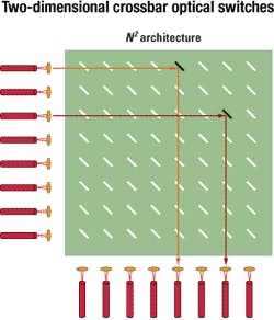
Underpinning the choice of technologies is an equally important consideration: the use of two-dimensional (2-D) versus 3-D architecture in the switching fabric. Bubble and liquid-crystal switch and crosspoint arrays use a fabric. In this approach, N input fibers are connected to N output fibers-a configuration that simplifies control electronics.MEMS can be fabricated in either 2-D or 3-D arrays. 2-D arrays typically are configured in a "digital" approach: Mirrors and fibers are arranged in a planar fashion, with pop-up mirrors moving between two positions. Controls are simplified, but scalability, as in bubbles and liquid crystals, is limited by the need for N2 components to accommodate a large number of ports. In a 2-D MEMS array, an 8x8 switch would require 64 mirrors.
As with bubbles and liquid crystals, the largest practical single array using 2-D MEMS technology is 32x32. Moreover, losses in 2-D devices vary with the length and course of the path that the light takes (see Figure 1).
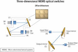
In 3-D MEMS arrays, mirrors can tilt in a variety of positions. Using a 3-D MEMS beam-steering architecture, signals are directed to an array of dual-axis mirrors that can be tilted in multiple positions, bouncing an incoming signal off one of the mirrors to another dual-axis mirror and finally to the designated output port (see Figure 2). The continuous-tilting feature of 3-D MEMS enables port counts to grow on a 2N scale, instead of N2-two arrays of N mirrors each are used to connect N inputs to N outputs.
3-D MEMS arrays are inherently scalable. Scalability is of paramount importance to carriers, who must be able to gracefully accommodate the rapidly accelerating growth in bandwidth demand. Carriers need to invest in a technology that has a future, enabling them to use the same supplier and integrate the same architecture as larger fabrics are needed and become available. The 2N design approach results in linear growth of crosspoints and components, making 1,024x1,024 and larger arrays practical using today's fabrication techniques. By contrast, an array of 1,000 crossconnects in a 2-D system using an N2 architecture would require one million mirrors.
2-D MEMS providers can use a Clos architecture to increase their number of ports by ganging together several low-port-count 2-D switch fabrics. However, this architecture inherently leads to a higher cost per port when compared to 3-D MEMS due to the increase in the number of switch fabrics used as well as the additional fiber-management issues involved.
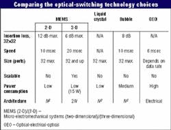
Combined with the extremely compact physical dimensions of the micromirror assembly, 3-D MEMS design enables the fabric to be scalable to very large crossconnect applications, using an SFF with relatively low power dissipation. What's more, 3-D MEMS arrays are inherently nonblocking, achieving "any-to-any" connectivity between all input and output ports and reducing path-dependent insertion losses that occur at each crosspoint in 2-D systems (see Table). Typically, as you increase the matrix size in 2-D, loss increases. For 3-D MEMS, however, loss for 64x64 is the same as 256x256-variation between the optical paths is minimal. In addition, the outlook for reducing losses is highly promising, moving from 8 dB in early devices to 4 dB (currently found in 64x64 3-D MEMS) and even 2 dB in the future.3-D MEMS technology is not limited to large arrays. Low insertion losses and SFF and power requirements make 3-D MEMS switches competitive with other technologies even in medium-sized and smaller applications-even as small as 8x8 arrays. Thus, system designers who select 3-D MEMS for their switching fabric can have confidence that their technological investment will be applicable across their networks.
The 3-D approach requires an "analog" system to drive the multiple positions of the mirrors, thus requiring circuitry that controls the focusing process and control algorithms to enable precise addressing and movement of individual mirrors.
One of the most important forward-looking elements in 3-D MEMS is the synergy with silicon IC fabrication. The ability to tap the immense learning and experience of IC fabrication techniques means that performance parameters will continue to improve, so that systems designers will be able to create networks that use lower-powered optics with fewer amplifiers. The use of the vast base of IC technology enables ever-greater integration of control electronics and other circuitry on the same fabric as the mirrors, enabling greater savings in space, power, and overall costs.
Silicon fabrication techniques also facilitate reliability, another critical consideration for network providers. MEMS arrays have undergone extensive, long-term testing, with mirrors successfully operated through their entire range of movement billions of times. Like 2-D MEMS, 3-D MEMS arrays will continue to be tested against Telcordia Technologies specifications and prove to meet the most stringent requirements of the communications and information industries.
The inherently forward-looking nature of 3-D MEMS is of special importance to network providers who need to maintain an unwavering focus on the future. 3-D MEMS represents a fundamental paradigm shift: using and manipulating wavelengths, rather than fibers, as the unit measures of bandwidth in today's 10-Gbit-and-higher systems. This capability enables network providers to provision, protect, restore, and manage bandwidth with far greater speed and simplicity than can be achieved using current approaches.
By creating a unique switching fabric that operates quickly and efficiently and is highly cost-effective and scalable, 3-D MEMS could vastly extend the reach of fiber-optic communication beyond core networks-even to the "last mile" of end customers in their homes and offices. The net result will be to help service providers generate more revenue by facilitating the offering of a wealth of new services and capabilities, provided to more people, more economically, than has been possible before.
Tom Albertson is a product marketing manager for Agere Systems (Allentown, PA).


