MEMS technology ushers in a new age in optical switching
There are two basic design approaches to MEMS optical switches; each has its advantages and drawbacks.
Marc Fernandez and E. Kruglic
Optical Micro Machines Inc.
The holy grail of the all-optical crossconnect is finally within reach. This year, micro-electromechanical systems (MEMS) technology leaped from the laboratory to the field in optical-switching applications. We've seen demonstrations of MEMS-based optical switches routing live data traffic. The promise of thousands of photonic data-channel ports switched-all optically transparent to wavelength, data-rate, and signal format-is imminent.
MEMS is a relatively new technology that builds complex machines so small that these systems are measured in microns. Although not widely publicized, MEMS technology has been deployed for over a decade in multiple applications such as airbag sensors (accelerometers), pressure sensors, displays, adaptive optics, scanners, printers, data storage, and micro-fluidics. Some of these micro-machines have gears smaller than motes of dust. Although many MEMS structures look familiar when viewed under a microscope, their function is governed by forces that do not affect traditional machines. Micro-machines are more subject to atomic forces and surface science than to gravity or inertia.MEMS devices typically combine electronic circuitry with mechanical structures to perform specific tasks. For optical switches, the key mechanical components are MEMS-based micro-machined mirrors fabricated on silicon chips using well-established, very-large-scale integration (VLSI) complementary metal-oxide semiconductor (CMOS) foundry processes.
Commercial MEMS-based all-optical switches are based on one fundamental principle and two well-understood approaches. The principle is simple: The switch routes photons from one fiber-optic cable to another. The routing is accomplished by steering the light through a collimating lens, reflecting it off a movable mirror, and redirecting the light back into one of N possible output ports.The two basic design approaches for translating this principle into optical switches are a two-dimensional (2-D) or digital approach (N2 architecture) and a three-dimensional (3-D) or analog approach (2N architecture). Each approach has advantages and disadvantages, but the combination of both in distinct but complementary product lines provides a comprehensive range of optical-switching solutions.
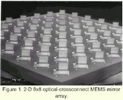
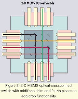
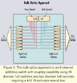
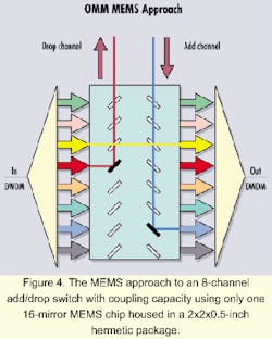
The 2-D digital approach is so-called because the micro-mirrors and fibers are arranged in a planar fashion, and the mirrors can only be in either of two known positions (on or off) at any given time. In this approach, an array of MEMS micro-mirrors is used to connect N input fibers to N output fibers. This is called an N2 architecture, because it uses N2 individual mirrors. For example, an 8x8 2-D switch uses 64 mirrors (see Figure 1). A big advantage of this approach is that it requires only simple controls, essentially consisting of very simple, transistor-transistor-logic (TTL) drivers and associated electronic upconverters to provide the required voltage levels at each MEMS micro-mirror.Apart from a robust product line of NxN switches, including 4x4, 8x8, 16x16, and 32x32 ports, which use an input and an output fiber port, the 2-D planar approach supports the introduction of a third and fourth fiber port to a basic NxN switch (see Figure 2). That permits dynamic add/drop functionality, arrays of 1xN switches in a single package, and customized mirror configurations on the chip. These features allow an array of mirrors to replace yesterday's cumbersome, expensive, custom discrete switch integrations (see Figure 3) with small, hermetically packaged, robust, custom switching configurations (see Figure 4).
Although the simple 2-D design is inherently flexible, the greatest challenge in this approach lies in scaling switching to very high port counts. As port counts double, the distance the light must travel through free space squares. As the pitch of the micro-mirrors increases, the light-propagation distance increases and the diameter of the light beam grows, placing tight constraints on collimator performance and mirror-alignment tolerance. Such a tradeoff can rapidly become unmanageable, leading to very large silicon devices and low yields. Because of the length of the travel path for the signal, as well as the angle tolerance and angle uniformity required on the MEMS mirror itself, 32 ports are currently considered a top-end size for a single-chip solution in 2-D technology.
This is not to say that a 2-D approach is limited to 32 ports. On the contrary, there are exciting architectures, including the well-known Clos approach, that cascade smaller 2-D switches into a multistage architecture scalable to hundreds by hundreds of ports. An example is Siemens's Transexpress MODIF optical service node.In a 2-D approach, insertion loss is primarily attributable to three distinct factors: The coupling loss of the collimating lenses, loss due to Gaussian beam propagation, and loss introduced by mirror angle divergence from 90 degrees. Additional factors are mirror angle uniformity across the array and travel distance variations along non-uniform path lengths. Despite these factors, Optical Micro Machines (OMM) demonstrated insertion losses averaging <5 dB for its 16x16 switch systems.
Another benefit of the 2-D approach is the ability to move rapidly from development to high-volume manufacturing, while maintaining the optical performance of a hand-built component, coupled with the reliability and cost-effectiveness of a mass-produced product.
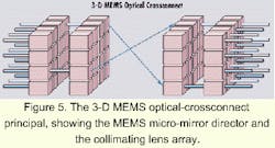
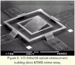
In many respects, the 3-D analog or beam-steering approach is actually very similar to the 2-D approach. It uses the same principle of moving a mirror to redirect light. The 3-D approach results in a 2N architecture, because two arrays of N mirrors each are used to connect N input to N output fibers (see Figure 5). But in this approach, each mirror has multiple possible positions-at least N positions (see Figure 6). This approach is much less constrained by the scaling distance of light propagation as the port count grows. Such architectures can scale to thousands by thousands of ports with low loss (potentially 6 dB or less) and high uniformity.
These advantages come at a price, however. Because the micro-mirror must have multiple possible positions, a sophisticated analog-driving scheme is implemented to ensure that the mirrors are in the correct positions at all times. Although MEMS technology can produce 2N 3-D mirror arrays with impressive stability and repeatability by using a simple open-loop driving scheme, closing the loop with active feedback controls is fundamental to achieving the long-term stability required in carrier-class deployment of an all-optical crossconnect. Using a closed-loop control scheme implies that monitoring the beam positions must be implemented in conjunction with computation resources for the active feedback loop and very-linear high-voltage drivers.
Of the many possible methods of actuating a MEMS optical switch, two have emerged as possible solutions for commercial optical products: electrostatic and magnetic.
The electrostatic method relies on the attraction of oppositely charged mechanical elements. It is one of the main actuation methods used for all types of MEMS devices. Its many advantages include repeatability, ease of shielding, and well-understood behavior.Magnetic actuation relies on attraction between magnets and typically one or more electromagnets. While magnetic actuation can generate larger forces with high linearity, the MEMS community generally has not taken to its use because of the complications of integrating the magnets and the near impossibility of shielding neighboring devices from actuator crosstalk. The shielding problem is particularly difficult in non-laboratory situations where, for example, someone might be running a large electric motor nearby, thus generating huge and repeated magnetic disturbances. Additionally, magnetic actuators on the MEMS scale have yet to prove reliable. Many developers are also concerned with hysteresis, both in the magnetic domain and in the structural properties of the magnetic materials.
The only way to ensure reliability is through long-term testing and field use. So far, electrostatic is the only mass-produced and fielded MEMS actuation method. For many years, a large amount of effort went into solving the problems of electrostatic behavior, and many products using electrostatic actuation have reached the market in demanding fields. A prime example is Analog Devices' electrostatic MEMS device found in most modern airbag systems. Modern electrostatic MEMS devices often have positioning accuracy measured in fractions of an angstrom (somewhat smaller than a single hydrogen atom), with reliability greater than that of the electronics supporting them.However, not everyone employs electrostatics due to its relatively low force potential. An appropriate structure combined with the right process is necessary to design structures that work well in this regime. If the structure is too stiff, for example, greater force may be needed, dictating the use of magnetic actuation. The MEMS designer makes tradeoffs, choosing either to accept the weaker forces of electrostatics or to fortify the system shielding and packaging and tackle the long-term reliability issues associated with magnetics. Because many open-ended questions remain in the use of magnetics, the electrostatic actuation method remains the optimum choice today for reliable devices required in high volumes.
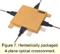
Even when designers employ electrostatic actuation methods, optoelectronic packaging remains a considerable challenge. The traits that make MEMS so well matched with optical switching-most importantly, small size-can also present some of the biggest obstacles in making MEMS devices robust and manufacturable. With the compact scale of MEMS structures, a drop of water can seem like a typhoon and a speck of dust like a landslide. To keep these potentially destructive forces from causing harm, it is imperative to hermetically seal the MEMS chips. One solution is to integrate the electronics of a MEMs optical-switch subsystem with the optics and micro-mirrors in the same hermetically sealed ceramic packages (see Figure 7). This integration radically improves reliability and drastically simplifies manufacturabilityBy internally packaging the optics, whether it is collimating lenses or waveguides, they become considerably less susceptible to shifting or misalignment due to environmental effects that can wreak havoc on exposed optical components. But if the manufacturing process is not closely controlled, the benefits of internally packaging optics and electronics with the MEMS switch can be offset by new vulnerabilities introduced by the need for multiple fiber feedthroughs through the hermetic package. Each fiber or pin entering or exiting the package represents a possible point of compromise to the package's hermeticity. Careful attention must be paid to this issue in the manufacturing process.
The key to controlling manufacturing processes and ensuring hermeticity in the high volumes required for current and future applications is the development of automation in manufacturing. The manufacture of the actual MEMS-based switch core exploits established, highly automated silicon foundry processes in use for more than a decade. The remaining challenge lies in fiber integration and module packaging.
Automation is crucial before, during, and after optoelectronic packaging of MEMS devices to reduce cost and cycle time as well as improve product quality and consistency. For example, consider the full optical-performance testing of a 32x32 optical crossconnect with over 1,000 possible paths. Using traditional manual testing methods, this type of testing can take more than a week. OMM has developed in-house test equipment that performs a full optical-performance test in just a few hours.
While these hurdles remain in the path of full-scale deployment of MEMS-based all-optical crossconnects, advances in optical and silicon technology bring us closer to the goal every day. In January, field trials at an unmanned central office marked the first time that optical switches based on MEMS subsystems were deployed to carry live data traffic. OMM delivered a custom-configured rack-mount optical-crossconnect subsystem containing 4x4 and 8x8 all-optical-crossconnect switches for field trials by the National Transparent Optical Network Consortium (NTONC) at a network node in Oakland. NTONC includes Nortel Networks, GST Telecommunications, Sprint Communications, Lawrence Livermore National Laboratory, and San Francisco Bay Area Rapid Transit (BART).
The optical switches worked flawlessly for the complete duration of the trials. Although a relatively new technology, MEMS-based switching must be held to the same high standards as any critical network component. The field trials established MEMS's high reliability and excellent optical performance. The new age in optical switching has arrived.
Marc Fernandez is the director of business development for advanced products, and E. Kruglic is the principal MEMs designer at Optical Micro Machines Inc. (San Diego).

