Programmable mixed-signal devices optimize fiber-optic communications links
Flexible control of modulation parameters can ease testing and speed production.
JOE CIANCIO, Xicor Inc., and REX NIVEN, Forty Trout Electronics
Good performance in a communication system, as defined by low error rate, depends on maintaining a high degree of separation between the different transmitted symbols as they arrive at the receiver.
Electronic systems using radio or copper links can use differences of phase, frequency, polarization, and amplitude in various combinations, including sub-carriers, to transmit symbols. When more degrees of freedom are used, the "distance" between the received signals can be increased so that they are more readily distinguished at low signal levels. However, in laser-diode transmission systems modulation, control of distortion and detection of parameters like phase or frequency (wavelength) are not yet sufficiently robust for commercial use.Thus, laser diodes must maintain adequate extinction ratios to ensure the clear transmission and reception of signals. Integrated circuits designed for control of laser diodes are available from a number of suppliers. With systems requiring ever more stable settings, however, digital potentiometers are now being used to calibrate equipment containing laser diodes at the point of manufacture. Digital potentiometers eliminate the need to manually adjust potentiometers after they have been through shipping or have endured changes in their operating environment.
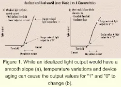
The laser diode transmitters commonly used in transmission have a characteristic threshold current (Figures 1a and 1b), below which no appreciable signal is produced and a steep curve where optical output power increases sharply. The "0" level is often set close or just above the threshold, which helps (among other reasons) minimize response time for the laser device. The "1" level is set at a point on the curve where the power level is close to the design value.
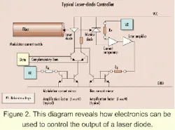
Due to temperature variations or device aging, this value can easily change, and typical systems use a monitor photodiode incorporated into the laser package to feed back to the controller a current representing the optical output signal. In many laser diodes, the threshold is large compared to the modulation current (difference between "0" and "1" drive levels), and this causes significant changes in optical power as temperature varies.As mentioned earlier, integrated circuits designed for control of laser diodes in this application are available from a number of suppliers, with digital modulation of the laser diode up to 1.2 Gbits/sec to comply with the gigabit interface converter (GBIC) standard. These circuits typically incorporate an input current to control the bias current (approximately the threshold or "0" current) and another to set the modulation current, which is added to the bias by a transistor pair controlled by the data signal (Figure 2).
For edge-emitter laser-diode devices, the threshold can be as large as the modulation current and can vary from device to device by a large factor-as much as 10. The modulation current can also vary considerably, typically by a factor of 5. Increasing operating temperature has significant effects on the laser diode:
- Threshold current increases considerably.
- Slope efficiency reduces (meaning the modulation current should increase to compensate).
- Coupling to the fiber or the monitor diode may change (effectively a change in the relationship of optical output to monitor-diode current known as "tracking error").
Vertical-cavity surface-emitting laser diodes typically have a much lower threshold with a different dependence on temperature.
The feedback loop using the average output of the monitor diode should cancel temperature variations of threshold and modulation current, but cannot separate the two, and for higher temperature, the feedback loop has the effect of reducing the extinction ratio (Figure 3).
Input from the monitor photodiode is used in a control loop (see Figure 2) to maintain the bias at the set level (typically another current input). Although an ideal system would detect output and control currents for "0" and "1" levels independently, the monitor photodiode can usually only discriminate an average power level with a time constant of several tens of nanoseconds at best. This time constant is usually much greater than a transmitted bit period, so the extinction ratio cannot be directly determined by the controlling electronics.
As it is important to avoid overdrive of the laser diode, it is prudent to include a safety margin of drive to allow for tolerances, such as temperature-dependent and time-varying parameters. Minimization of the safety margin by tight control of these parameters translates directly to increased extinction ratio.Setting of the control currents can be made by fixed resistors (RM, RB, RP) between the controller and an integrated reference voltage, as shown in Figure 2. The value of the reference can be made to vary in sympathy with temperature-induced variations in the control current input voltage.1 This is typically that of a current-mirror base-emitter (or gate-source) voltage drop, and the input voltage will vary considerably with temperature. Due to the large tolerances in the laser-diode characteristics of threshold, and to a lesser extent, current optical power-conversion efficiency, the resistors in each module must be set-on-test for each unit.
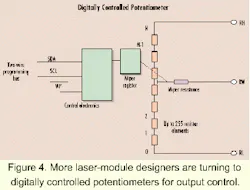
The drive toward automation in manufacture and test processes leads to a requirement for programmable and flexible resistors and other laser modulation control devices. An ideal way to make modulation adjustments is with "set-and-forget" digitally controlled variable resistors and potentiometers (DCPs). The reliability of the settings DCPs provide can exceed that of mechanical potentiometers and results in a consistent setting that is essentially tamper-proof in the end application. DCPs allow setting of a "tap" in a linear array of resistors, programmed via a two-wire bus, with settings held in an internal EPROM for recall at power up. These are configured like a potentiometer but can also be used as a programmable variable resistor (Figure 4).
The wide range of threshold necessitates a large number of possible resistor values. For example, a DFB device having an initial threshold current that varies over a range of 5 to 50 mA, for which we want to set the current within ±5% of the ideal value, requires a resolution of 0.5 mA at the high resistance (minimum threshold current) end, and 5 mA at the low resistance end. Assuming a nominal control voltage of 1.25 V and a current amplification ratio b of 40, this means a minimum resistance element of 2x(5%)(1.25 V/50 mA)*b = 100 ohms, but with a maximum value of (1.25 V/ 5 mA*(b) = 10,000 ohms. Therefore, 100 equal-sized elements of 100 ohms each would be necessary.A new DCP now on the market contains two arrays, one of 99 elements and one with 63 elements, with a total resistance of 10k, and another of 255 elements (total resistance of 100k) normally used to set the desired monitor-diode current (RP in Figure 3). The second 63-element, 10k device can be used to achieve higher resolution, or to set other parameters such as modulation level (resistor RM), output level, or device temperature.
Adjustment of the laser-diode device temperature offers a means of compensating for wavelength change that may occur as bias currents change. This could be important in WDM systems.
Should the resistor values available not be well suited to the laser-diode device being used, the alternative arrangement of using the device in potentiometer mode gives a very wide range and virtually no temperature coefficient due to the resistor.
Tap changes of the DCPs are always made in make-before-break manner, thereby avoiding large momentary changes of the control-loop parameters when active-trimming.
With the architecture of Figure 3, the main causes of drift are:
- Changes in the optical coupling between the laser and monitor diode, and laser and output fiber.
- Change in the reference current through RP, typically due to temperature.
- Saturation of the feedback loop.
The first cause is specified by the laser device manufacturer as a tracking error with a typical value of 0.5 dB max. (12%) over the working temperature range.
The second is a function of the reference voltage but also of the resistor stability. The programmable resistor devices have a temperature coefficient of up to 300 ppm/°C, or a drift of less than 1% even in an extreme case of a temperature change of 30°C.
The third can be avoided by proper understanding of system parameters at the outset and by having adequate resistance range and resolution in adjustments.
Enhancements to DCP technology allow more than just the digitally controlled adjustments; advances in integration have also allowed incorporation of programmable trip levels on voltage monitors that allow (for example):
- Detection of excess optical power level for laser device reliability and eye safety.
- Reporting when the optical signal falls below a minimum level.
- Monitoring of system power voltage.
- Control of device temperature.
These may also be linked to an alarm or a rapid-shutdown circuit to prevent damage to the laser device. These threshold voltages are programmed as analog voltages that directly charge a memory cell, giving 25-mV resolution, with very-long-term retention.
With a controller connected permanently or during maintenance, corrections such as those to correct device aging can be made dynamically, since the technology allows up to one million memory writes, with 100-year minimum data retention.
Nonvolatile EPROM memory is also available for storing serial numbers, fiber-optic component values, calibration dates, and so forth. Different parts of the device are written by using different internal addresses. Integrity of this data is assured by a requirement to enable writing as a separate instruction, as well as asserting a write pin before the memory can be altered. In addition, each byte of data successfully received is acknowledged by the circuit by pulling low the bi-directional data input at a particular moment in the cycle.
The device is expected to be incorporated into hot-swappable modules. Further, power-management features have been provided, including monitoring of power-supply voltage and programmable timing period after supply voltage is within spec before power is considered stable.
An important advantage of this integrated approach is the small size of the package available. A ball-grid-array format option requires a footprint less than 5 mm x 5 mm. With laser-diode controllers available in fine-pitch packages such as TSSOP, the printed circuit board area required for a fiber-optic interface can be less than 10 cm2.
- Micrel, "Synergy Semiconductor Data Sheet SY88905", Rev B Amendment 0, December 1998, p. 5-682, characteristic for Vpinset voltage tracking.
Joe Ciancio is a product-development engineer at Xicor Inc. (Milpitas, CA). Rex Niven is managing director, Forty Trout Electronics, a design consultancy in Australia.
In fiber-optic data transmission and free-air infrared communication, as specified by the Infrared Data Association (IrDA), it is common to use a simple on-off keying (OOK) where, for example, a "1" is a burst of carrier (light) and a "0" is represented by a low signal level.
At reception, the detector converts this to an electrical signal with associated noise due to the transmitter, the optical path, including amplifiers, and the receiver. The "1" signal would classically be represented as a mean value with a Gaussian distribution of noise. The zero signal is a little different, since "negative light" does not exist; therefore, all optical noise is detected on the "1" side of the distribution. This means that for a given level of noise, a ratio of signal-to-noise even greater than the classical values for binary communication systems is required, especially where optical amplifiers or photomultiplier detectors are used.
Assuming amplifier noise is already minimized, this suggests that the extinction ratio (or ratio of detected "1" to "0") is a key parameter in minimizing bit-error rate (BER).
If you have an idea for a feature story or would like to contribute to Lightwave, please contact Editorial Director Stephen Hardy at tel: (603) 891-9454 or e-mail: [email protected]. Ideas must focus on topics related to fiber optics and optoelectronics in the communications industry.


