Hollow-waveguide technology cuts cost of integrated optical components
When he joined Qinetiq as product manager, telecommunications, in late 2001, James McQuillan was asked to develop the business potential of the company's R&D capability. Qinetiq is a Malvern, UK-based former Ministry of Defence R&D organization, now freed from the ministry's control and one-third owned by Carlyle Group. One project that caught McQuillan's eye was a new component assembly and manufacturing technique called hollow-waveguide (HWG) technology, in laboratory development under Mike Jenkins, technical leader and Qinetiq Fellow in the Photonics Business Group.
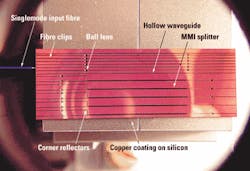
HWG technology combines a patented low-loss auto-aligning waveguide technology with standard manufacturing processes. According to Qinetiq, it delivers in excess of 60% reduction in device manufacturing costs, depending on the application. It also allows relaxed alignment tolerances and easy integration of monolithic functions—effectively for free. Says Jenkins, "Our selling line is that this technology is the optical equivalent of the electronic circuit board."In an HWG-based integrated optical device, the paths between lasers, active or passive devices, filters, switches, and so on, are open-air-filled channels, typically 50 µm wide and carved out of the device substrate by deep reactive ion etching. This structure offers several advantages over the solid-core waveguides typical in other integrated devices.
With solid-waveguide structures in gallium arsenide, there is often significant difficulty in aligning guides and devices because the waveguides are so small, typically 3-4 µm across. Index-matching gel is usually required too. The other main alternative—a free-space solution—suffers problems of divergence and diffraction.
At the start of HWG's development, Jenkins had been working with 10.6-µm devices for radar-type applications. However, to take the technology to optical communications application, the principle was adapted to suit 1550-nm devices. "At OFC 2003, we spoke to quite a few people from some of the biggest players across optical-component development from North America, Europe, and Japan. Everybody we talked to said that they could see that HWG technology would enable component assembly in a better way," says Jenkins.
Qinetiq has partnered with Atlanta-based Engent (Engineering Next Generation Technologies), a 51% subsidiary of Siemens. Engent, with whom Qinetiq is signing a letter of intent, can manufacture and assemble up to 1,000 ball-lensed fibers into HWGs per hour. As with any micro-electromechanical system (MEMS), it is possible to simultaneously make the MEMS and the MMI devices. Typically, the HWG material is silicon and there is a choice of metallized coatings such as gold or copper.
"There's a subtlety to this process," explains Jenkins. "Companies haven't been doing this previously, because people who make solid-core waveguides always think that they have to make them to singlemode dimensions."
HWG waveguide specifications include typical losses (and polarization-dependent loss) of <0.1 dB/cm.
"We are now offering a low-risk access to HWG technology based on Qinetiq's technology and Engent assembly process expertise," notes Jenkins. "Together we are working to develop manufacturable designs, prototype assembly, and achieve pilot production of devices before transferring that into customer premises."
HWG-produced integrated optical devices offer significant cost savings in manufacture. For an eight-port reconfigurable optical add/drop multiplexer, for example, featuring eight thin-film filters, eight variable optical attenuators, and eight switches, the cost would normally be about $6,560. With HWG technology this subsystem would cost $1,936—a 70% savings. Qinetiq is now looking at the application of ballistic-missile technology to optimize Engent's pick-and-place process to take obstruction and position into consideration.
Matthew Peach is editor-in-chief of Lightwave Europe.

