Optical MEMS: Offering cost reduction for telecom systems
A large number of optical MEMS devices have been developed the last few years, but only a few will find their way to high volume, thanks to cost-effective manufacturing and packaging using a modular and flexible systems approach.
James Aberson, Colibrys, and Patric Salomon, 4M2C
Optical components are key elements in telecommunications networks, but operators need to reduce investment and operating cost, manage increased systems complexity (mainly due to DWDM technology), and reduce their inventory. Solutions to these challenges can be found in using tunable components to replace fixed-wavelength components (lasers, filters, etc.), reduce manufacturing cycle time to respond to the cyclic nature of the industry, and promote different ways of saving space (i.e., reduction in fiber splicing and integrating more components and intelligence in a single optical module).
Several of these trends will be supported by micro-electromechanical systems (MEMS) components and structures.
Integrating optical functions and modules
Obviously, the most significant trend in MEMS technology today is the integration of multiple optical functions into a single chip or module. Hybrid integration is the first choice for today's volumes, but with the move toward high-volume applications, monolithic integration will be the long-term aim to achieve even better cost reduction. More functionality on the same chip can be realized by integrating planar-waveguide circuits with arrayed-waveguide gratings, detectors, and amplifiers.
Another approach in lowering cost is to aggregate demand for non-telecom and telecom applications to increase production volumes of micromachined components and decrease costs over all markets. In other words, the design of optical MEMS components in a "micro-brick" manner will open uses in products that are outside the main telecom roadmap. Assembling these optical MEMS building blocks in innovative ways could address new areas like micro-displays and micro-sensors for medical, physical, and environmental applications.
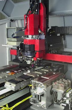
The replacement of costly hand assembly with precision robotics will be another major milestone, maybe even the most important one, in cost reduction. A variety of rather generic manufacturing platforms are under development, but most solutions used so far are still being developed on a customer-specific basis. Figure 1 shows a precision assembly robot system used for the assembly of lasers, diodes, lenses, MEMS chips, and fibers. Accuracy with passive alignment of ±2 µm and with active alignment of even ±0.1 µm could be achieved using the system. In the production process, a high throughput of typically 30 modules per hour was reached with exceptional repeatability and guaranteed quality.
Toward optical hybrid manufacturing
Optical hybrid technology is expected to become a standard technology in much the same way as electrical hybrids. It is a key element in meeting the cost-reduction requirement for the next generation of optical telecom products. Standardized automated assembly platforms allowing for higher integration and tunable/reconfigurable modules are the solutions being sought.
Companies that want to build an optical hybrid technology platform need to design the basic platform technology and design/adapt components to fit the platform. The diversity of assembly technologies should be reduced toward a standard approach applicable to a large class of components. Assembly platforms should fit into low-cost electronics packages and solve the complexity issue of integrating a growing number of functions in the same package.
Standardized interfaces between components, substrates, and assembly tools need to be established. All these different technologies need to be pulled together and adapted with three key requirements in mind: cost, functionality (precision, stability, complexity), and reliability.
Alignment and fixation using MEMS structures
MEMS silicon optical benches, optical-fiber attachments using passive MEMS V-groove alignment or other geometries of MEMS-based passive alignment and fixation structures, are good examples of hybrid technology platforms. For fiber assembly, technologies like silicon V-grooves, mechanical clips, and fusion of fibers to lenses are already used in industry.
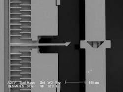
As shown in Figure 2, micromechanical fixation structures fix fibers and lenses as an integral part of MEMS micro-shutter devices. This kind of technology can avoid the typical approach whereby components are first fixed with micron accuracy, then fine-tuned through costly active realigning and laser hammering. In these approaches, soldering and laser welding can replace glues to achieve more stable and reliable mechanical strain relief.
Foundry business model
Cooperation between traditional telecom component/system companies and MEMS providers will be another clear trend in lowering optical-system costs. "Open foundries" undertake custom designs directly for customers, depending on application. A flexible MEMS foundry is able to adapt to requests from the systems level quickly and can achieve the desired cost savings with its large portfolio of underlying MEMS technologies. Fast time-to-market and lower cost per component can be achieved through the cooperation of a flexible MEMS foundry and telecom component/systems manufacturers.
There is little doubt the telecom arena will soon resume expansion at a staggering rate on a worldwide scale. MEMS will play a crucial role in enabling this expansion. The current downturn opens opportunities for innovative technology providers to reassess microtechnologies and gain market share once the systems providers need to invest again.
James Aberson is business development manager at Colibrys Inc. (Cary, NC), and Patric Salomon is managing director of 4M2C (Berlin). They can be reached at [email protected] and [email protected] or at the Colibrys booth (#7849) at OFC 2003.

